Basic EMI Pre-Compliance and Troubleshooting Techniques
450 likes | 556 Views
Learn basic EMI measurements and analysis, including radiated and conducted noise sources. Discover how EMI is coupled and measured in equipment, with a focus on LISN networks and measurement filters. Develop skills for pre-compliance testing and troubleshooting strategies for efficient problem-solving.

Basic EMI Pre-Compliance and Troubleshooting Techniques
E N D
Presentation Transcript
Basic EMI Pre-Compliance and Troubleshooting Techniques C. R. Swartz, Senior Principal Engineer/Manager
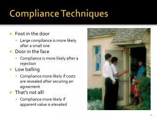
Overview • Basic EMI Measurements and the LISN • Common and Differential Noise Sources • EMI Pre-Compliance Analysis Using Simulation Models • Layout Considerations • Field Probes, Signal Splitters and Simple Current Probes • An Extensive Troubleshooting Example Case History
Foreword If you work with Power Electronics, sooner or later you will need to know something about EMI. It is better to learn about it sooner and prepare for the day when you may have to solve a difficult problem. Often the problems will not happen at the most convenient time nor will you have the luxury of extended time to learn how to solve the problem. If you begin to think about it early in the design phase and design for it, you will develop tools that will someday allow you to respond quickly and solve the problem or recognize the problem before it becomes one. I hope you enjoy the material…………..
What Is EMI? • EMI stands for “Electromagnetic Interference” and it has been used to describe many different types of noise phenomena observed in modern power electronic systems in use today. • The term “interference” is used somewhat loosely today. Interference means that one piece of equipment’s actual operation is disrupted by either another piece of equipment or an external signal source. Actual interference is not usually implied by the term EMI unless describing a prevention device, method or test. • The two basic types of EMI are: • Radiated EMI; measured in the far-field using antennas • Conducted EMI; measured at the power entry port using a line impedance stabilization network (LISN) • There are two general categories of Conducted EMI (the focus of this seminar): • Differential-Mode Noise (sometimes referred to as Normal Mode) • Common-Mode Noise
How is EMI coupled? There are four basic noise-coupling mechanisms in electrical systems Conductive caused by direct contact with metal conductors (ripple or grounding issues) Capacitive caused by fast-changing voltages applied to capacitance between conductors Inductive caused by fast-changing currents flowing in a loop (transformer action) Radiated caused by far-field electromagnetic coupling (antenna effect)
How is conducted EMI measured in commercial equipment? LISN – Line Impedance Stabilization Network Copper Ground Plane Tied to Earth Ground
Power Source Unit under test power supplied here High-frequency chokes L1 and L2 block high-frequency noise from the power source. C6 and R7 along with C1 and R8 form high-frequency shunts to keep high-frequency noise from the power source from entering measurement of the EUT (equipment under test) The Line Impedance Stabilization Network (commercial products) LISN – Line Impedance Stabilization Network
The LISN impedance plot (simulated) Impedance approximates 50 Ohms from 150kHz to 30MHz, the measurement standard for conducted EMI. The LISN will vary depending on the measurement standard but the goal is a flat impedance in the area of interest Impedance (Ohms) I Impedance (Ohms) = V/I V Frequency (Hz)
Measurement Filters There are several measuring-filter techniques that you should know about: Peak Detection This method is the fastest of all EMI scans. It also generates the highest amplitude results. An envelope detector is employed that can respond very quickly to amplitude changes in the envelope but without the ability to track the instantaneous value of the input signal. Quasi-Peak Detection This detection method is a form of weighted averaging that has a fast rise-time constant but a slow fall-time constant. Narrow duty cycle signals will measure a lower value than peak but as frequency or duty cycle increases, the measured value will start to approach peak detection. Quasi-Peak detection takes the longest of all EMI sweeps. Quasi-Peak Detection has higher limits to allow for an “annoyance factor” of the offending signal. Average This method is peak detection followed by a filter with a bandwidth that is lower than the resolution bandwidth. The result is that the higher frequency peaks get averaged to a lower value. Average detection is slower than peak but faster than quasi-peak.
Differential-mode noise (A.K.A. normal mode) • Differential-mode noise is sometimes referred to as Normal-Mode noise. There is a good reason for this. It results from an applied voltage differential (of opposite polarity) between the noise source and the noise return. • It can be caused by any or all (hopefully not!) of the four coupling methods previously discussed • Normal circuit operation is also differential in nature • Differential noise requires only two wires or a single wire and ground • Differential-noise currents flow in opposite directions in input feeds or AC line and Neutral • Input voltage ripple, output voltage ripple are common examples of differential-mode noise • Differential noise appears in all forms of power feeds: both two- and three-wire feeds
This ripple current is responsible for the differential-mode EMI that will be measured at the LISN. We are concerned about these ripple currents, as they are responsible for the ripple voltage measured at the node Vin. This ripple voltage is the source for the differential-mode EMI that occurs at the fundamental as well as the much of the harmonic content. Differential-mode noise ideal CCM buck converter model SIMPLIS Consider the open-loop 12V – 3.3V ideal buck converter shown
Add our LISN equivalent circuit Differential-mode noise ideal buck converter To generate the noise model, we modify the circuit as shown below:
Common-mode noise • Common-mode noise always flows in the same direction in both input feeds (L and N) from an applied voltage between those common lines and earth ground (chassis, baseplate, test equipment, etc.) • It can be most difficult to determine the path since it can involve virtually any equipment connected to earth ground. • Earth ground or a three-wire system with an isolated ground is required. • Non-isolated DC-DC Converters need not have much consideration for common-mode noise (sometimes!!). • Test equipment can be very vulnerable based on the type of circuitry being measured. • Isolated converters that connect output (-) to earth ground will have common mode + differential-mode ripple at the output. • Common-mode noise can cause problems with non-isolated DC-DC converters if grounded test equipment has high common-mode noise flowing between them.
If we do nothing, the return path must be through the mains and LISN! Common-mode noise origin – isolated full-bridge topology
The current that passes through the LISN is the common-mode voltage measured from each line to ground divided by the LISN impedance. The common-mode voltage is the source for the common-mode portion of the EMI. Common-mode noise origin – isolated full-bridge topology The actual measured EMI spectrum will consist of common-mode + differential-mode currents. There will be some cancellation that occurs and also some additions.
When does a buck regulator generate common-mode noise? • Consider the simplified Buck regulator circuit shown below connected to an electronic load • It is powered from a LISN and set up to measure EMI. Can anyone find a common-mode EMI source?
When there is parasitic capacitance to earth ground Voltages at LISN that are in phase with respect to earth are common mode, out of phase are differential-mode EMI Noise source is output ripple! Current through parasitic capacitance shows up at LISN as in phase voltages when measured across each 50 Ohm port to earth ground!
Layout Matters! • Up to now, we have been simulating and discussing ideal layout filters. No layout is ideal. Most layouts are a compromise as there are many resources requiring the PCB area. • Parasitic inductance will limit the high-frequency performance of capacitors when it appears as ESL! • The layout can make your filter require more stages if it is not done to optimize the performance of the filter. • Two-sided PCBs without a dedicated ground plane can be the most difficult to achieve optimum filtering. • You can also model inductance and resistance of each interconnecting via and trace. • Extraction of parasitic inductance and resistance is very important to understand potential EMI sources (ringing) and the overall performance of the EMI filter.
To PCB Layout… Copper strap link for PGND PGND HS MOSFET Drain PGND L1 The parasitic paths around the loops must be considered in your final simulations and analysis or you will find the filter attenuation will not be as accurate. Use the ideal filter schematic to generate a first pass result, then modify it as the layout progresses to better account for the actual layout. Q1 VIN
Tools – Beehive 100 • Includes wideband RF amplifier and cables • Three H-field probes and one E-field probe • 100D is the E-field probe to the far right • Buy as a kit, a must have! Use the amplifier for the small field probes as they are less sensitive. The bigger probes allow you to find the approximate area of the offending signal while the smaller ones let you trace it more closely.
Tools – power splitters • ZSCJ-2-2+ Mini-Circuits • Blocks Common-Mode • ZSC-2-2+ Mini-Circuits • Blocks Differential-Mode • Both require dual or two single LISN(S) • Must use matched equal-length coax cables. Length should be as short as possible LISN-L LISN-N LISN-L LISN-N Analyzer Analyzer Signals out of phase are attenuated Signals in phase are attenuated
Tools – Swartzomatic-1 • Hand-wound HF current probe • Measures CM and DM current • High-permeability core • 50 Ohm cable • Wide BW, high sensitivity • Much better for high-frequency current with very low amplitudes than traditional current probe. Pass wires through core in same direction to measure common-mode current, opposite directions for differential current.
Tools – Swartzomatic-2 • Hand-wound near-field probe • Helps find high H-fields on PCB • Hand-made using RG-58U • 50 Ohm cable • Common-mode beads can be added to cable as an option Connect to 50 Ohm termination on scope. Start with higher volts/div while moving around PCB. Then reduce volts/div to allow location of near-field to be determined. Then use lower sensitivity probes (Beehive) to trace offending H-field caused by noise currents of interest. Makes an excellent trigger without connecting to circuit.
Troubleshooting – design challenges • 250W+ Critical Conduction Buck Regulator • Efficiency had to be 96% or higher, high switching frequency 700kHz • PCB area was small, isolated metal box enclosure, potted. • High ambient environment up to 65°C • Thermal Management • Power SiP and PCB needed thermal connection to plate for cooling • This caused less-than-optimal ground plane, increasing parasitic inductance • CISP25 Conducted EMI • Required two-stage filter as second harmonic needed –40dB attenuation
Tools – at my disposal • An excellent simulation model of powertrain and filter design • Performed AC and transient analysis of power system with filter, no issues • Performed parasitic extraction of layout after it was done. • Test Equipment • All tools shown previously plus Spectrum Analyzer and Oscilloscope. • LISNs, differential amplifiers and a good network analyzer.
Troubleshooting EMI – the filter used The EMI filter is shown below (idealized) for purposes of illustration EMI DM noise source EMI is measured across each 50 Ohm resistor to earth ground High-amplitude, high-frequency AC current “sloshes” around in this loop. The voltage developed across it is the differential-noise source the filter needs to attenuate
Troubleshooting EMI – the initial measurements High-frequency EMI was totally unexpected. The only thing that matched expectations was the fundamental. The initial measurement spurred my work on a new book entitled “What You Thought You Knew About EMI” !! EMI is measured across each 50 Ohm resistor to earth ground
Troubleshooting EMI – the initial measurements DM signal measured at SiP input on customer board: high frequency (6 – 10MHz) is higher by 8 – 12dB, a noticeable ringing observed DM Signal measured on evaluation board with better ground plane
Troubleshooting EMI – the ground plane differences PGND Customer layout MID-1 Input capacitors Input capacitors VIN is major heat source. Needed to be carried through all 4 layers in customer design to form robust pad to thermally bond to plate. Notice the large amount of via’s needed to carry the heat load through the board to the plate. Ground plane is broken up. Evaluation board top layer Evaluation board MID-1 layer Notice ground plane is only broken by a small number of vias with flooded copper around them. Much lower parasitic inductance but thermal impedance is too high to meet thermal requirements. Input capacitors
Troubleshooting EMI – what I know and don’t know – what next? • The measured EMI at input to SiP shows significant high-frequency ringing in the area where EMI is failing. • I believe this ringing to be caused by layout – result of higher parasitic inductance and higher Q noise loop • How does this frequency get through the EMI filter? Is Filter deficient somehow? • Is the noise bypassing the filter? • Near-field contamination by high flux in inductor? • Capacitive coupling due to high-voltage transitions? • Radiated EMI into LISN? • Common-mode noise or differential-mode noise?
Troubleshooting EMI – next steps Determine if noise is CM or DM… EMI is measured across each 50 Ohm resistor to earth ground Added power splitters between LISN and spectrum analyzer. Blocking CM noise showed no change to high-frequency measurement. Blocking DM noise knock all high-frequency emission down by 30dB. Conclusion: Offending signal is differential
Troubleshooting EMI – next steps Determine which parts of EMI filter are working properly... Use diff-amp to measure this voltage. Take FFT and measure attenuation of first stage filter. - Does it match simulated expected results? Yes! First stage appears to work as designed. Use diffamp to measure this voltage. Take FFT and measure attenuation of second stage DM filter.- Does it match simulated expected results? No! 8MHz and other high-frequency noise here. No correlation to simulation whatsoever.
Troubleshooting EMI – next steps Open circuit and use network analyzer to sweep both filters. - Does attenuation appear as shown in simulation to be close? Yes! First and second stage filters appear to work properly small-signal-wise. Check simulation model of second-stage filter. Was anything missed like self resonance of inductor core? Remove 48V and short circuit input to LISN
Troubleshooting EMI – next steps 1. Highest H-field is inductor. Good starting point. - Any evidence of 8MHz ringing here? No! No evidence here or output capacitors. 4. Probe C17-C19. 8MHz and other frequencies detected! Next, vary the line voltage. - Does the EMI amplitude go up with line going up? If so, it may indicate capacitive coupling. If EMI varies with load, H-field coupling would be suspected. In this case it varied with load only. Use field probes to isolate where contamination is coming from 2. Probe around each capacitor in high AC loop and SiP. - Any evidence of 8MHz? Yes, around each capacitor and slightly higher around SiP 3. Probe around each capacitor C2-C6 and around L2.- Any evidence of 8MHz? No evidence. Very quiet here.
Troubleshooting EMI – fix layout Problem area isolated and fix implemented Fix implementation Area of suspected coupling 8MHz detected here with near field probe
Acknowledgements • The following material was used as references in the presentation : • Controlling Conducted Emissions By Design by John C. Fluke (an excellent book, highly recommended) • Predict Differential Conducted EMI with a SPICE Simulator Christophe Basso; April 12, 1996 • Making EMI Compliance MeasurementsAgilent Technologies Application Note • CISPR 22 Fourth Edition
Thank you Questions? The information contained herein and presented by Vicor is for general informational purposes only. Vicor assumes no responsibility for inaccuracies, errors or omissions in this presentation. Users of power supply products remain responsible for the design, testing and operational safeguards related to such use.