Download
1 / 87
880 likes | 1.16k Views
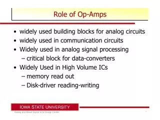
Role of Op-Amps. widely used building blocks for analog circuits widely used in communication circuits Widely used in analog signal processing critical block for data-converters Widely Used in High Volume ICs memory read out Disk-driver reading-writing. New challenges in Analog Design.

E N D
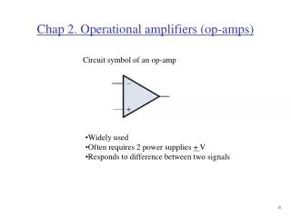
Role of Op-Amps • widely used building blocks for analog circuits • widely used in communication circuits • Widely used in analog signal processing • critical block for data-converters • Widely Used in High Volume ICs • memory read out • Disk-driver reading-writing
New challenges in Analog Design • Decreased Supply Voltage • Increased Digital/Analog Interference • Reduced Testability • Increased Parametric Variations
Critical Specifications for Op-Amps • High DC Gain • High Speed/Large Gain-Bandwidth • Sufficient Output Swing • High power efficiency Desirable: digital built-in-self-test and self-calibration
bias3 M4 M4 bias2 M3 M3 bias1 M2 M2 Vi1 M1 M1 Vi2 cmfb Mb Existingstructures&Limitations Cascode Amplifier DC Gain: Modest Speed: Excellent Power Efficiency: Good Frequency Response: Good Output Swing: Small
CP1 in A1 A2 A3 out CP2 Existing structures & Limitations Cascaded Amplifier DC Gain: High Output Swings: Large Frequency Response: Poor Speed: Poor
Vbp Vbp Vo2 Vo1 Vi1 Vi2 Vbn Existing structures & Limitations Positive Feedback Amplifier DC Gain: Large Speed: High Output Swing: Good Frequency Response: Good Low Yield
Our Objective • Low Voltage Compatible • High DC Gain • High Speed • Good Output Swing • High Yield • Standard Digital Process Compatible • Good Power Efficiency
Our Approach • Find new amplifier architectures • Rely on digital logic to enhance performance • Use simple digital circuit sensing amplifier performance • Integrate controllability • Use adaptive feedback control
Positive Feedback Gain-Boosting • Can operate at very low voltages • Can achieve very high DC gain • No compromise in bandwidth • No appreciable power increase • Conventional wisdom has two concerns • positive feedback leads to RHP poles • gain boosting is limited if requiring robustness w.r.t. process variations
Our response to the concerns • positive feedback causes RHP open-loop poles, but do not necessarily cause RHP closed-loop poles! • RHP open-loop poles can actually improve performance of closed-loop amplifiers! • F16/F18 fighter jets have open-loop RHP poles, they play critical role in achieving their superior closed-loop performance • no need for robustness across process variations • use positive feedback pole control after fabrication
Positive Feedback Operational Amplifiers Open loop transfer function Closed-loop transfer function Open-loop pole: Closed-loop pole:
Positive Feedback Amplifier Architecture Exploration • Some positive feedback amplifier architectures have a dc gain that is much more sensitive to the feedback control variable than others • Although architecture optimality may be difficult to determine, synthesis techniques may yield better structures than those already considered • Comparative study of several structures with existing positive feedback structures
M2 Vbias1 Vo gm1 A ADC = Vxx Mn gds1+gds2- (A-1)gdsn M1 CL AVo Vi Negative Output Conductance Op Amp Vdd As (A-1)gdsn→ gds1+gds2, ADC→ ∞ !
ImplementationBlock Diagram First Stage Negative Conductance Generator Vi+ Vi- 2nd stage Vip Vop Basic Amp CMFB Vin Von 2nd stage Bias Generator
M3 VBP M4 M9 M8 Von Vop Vout M1 M2 Vip Vin M7 Vin M5 M6 VBN VCM Basic Amplifier and the Second Stage Second stage Basic amplifier
Negative Conductance Generator Vdd M3 M6 M7 M2 Vi+ Vi- Mg2 Mg1 Mn2 Mn1 Vctrl Vctrl M5 M4 M1 M8 A VXX VXX Von Vop
Ma7 Ma3 Ma4 Ma5 Ma1 Ma2 Vop Von Vin Vip Ma8 Ma6 Ma9 VBN Low Gain Stage A
Positive Feedback Amplifier Architecture Exploration M3 f1(-θ1VA-θ2VB-θ3VOUT) VB M4 f2(-θ4VA-θ5VB-θ6VOUT) VOUT M2 f3(-θ7VA-θ8VB-θ9VOUT) VA M1 VIN Overhead for realizing this structure can be very small
M4 M4 bias2 M3 M3 k bias1 M2 M2 Vi1 M1 M1 Vi2 Mb Example positive feedback amp1: Gain = infinity
M4 M4 bias2 M3 M3 bias1 k Vo1 Vo2 M2 M2 Vi1 M1 M1 Vi2 Mb Example positive feedback amp2: Gain = infinity
M4 M4 bias2 M3 M3 k bias1 M2 M2 Vi1 M1 M1 Vi2 Mb Example positive feedback amp3: Gain = infinity
M4 M4 bias2 bias1 M3 M3 k M2 M2 Vi1 M1 M1 Vi2 Mb Example positive feedback amp4: Gain = infinity
Preliminary Results: DBISTSC PFAmp A Digital Programmable Amplifier Bifurcation in Positive Feedback Amplifier Simulation and Measurement Results
VDD M2 M2 CL CL Vo2 Vo1 Vi1 Vi2 Vbn VSS A digital controllable Amplifier • Low-Voltage Compatible • 3 transistors from VDD to VSS • High Gain • Attenuator provides positive feedback • negative-conductance compensation • High Speed • Single Stage
y x gmnx gon gop -gmpy sCL =0 Small Signal Linear Equivalence
Nonlinear Dynamic Dynamic equation Equilibrium manifold (DC Transfer)
0.02 0.021 0.03 Amplifier’s DC Characteristics y 0 x
y =0.021 x Amplifier’s DC Characteristics y =0.03 =0 0=0.02 L
0 No Hysteresis >0 Hysteresis Hysteresis Decrease L Gain Observations
y 1 ¯ 0.8 stable 0.6 0.4 ¯ 0.2 m m stable unstable 0 ® 0 -0.2 -0.4 ¯ -0.6 stable -0.8 -1 0.017 0.018 0.019 0.02 0.021 0.022 0.023 Phase Diagram in Y- Plane x=0
Phase Diagram in Y- Plane y *x=-0.001
Phase Diagram in Y- Plane y *x=0.001
0 No Bifurcation For a given x, one unique solution for y >0 Bifurcation For some given x, 3 solutions for y 2 stable and 1 unstable For some given x, one unique solution for y Observations
Pull up/Pull down Circuit pullup pulldown
Pull down, stay low Pull up, stay high Pull up/Pull Down y OHOL=10 x
Pull up/Pull Down Pull up, stay high y OHOL=11 Pull down, return high x
Pull up/Pull Down Pull up, return low y OHOL=00 Pull down, stay low x
pull up release record OH pull down release record OL 10 11/00 OHOL=? no bifurcation bifurcation detected Sensing Process
M2 W2/L2 Vi Vo 1. 2. M1 W1/L1 Linear MOS Attenuator 3. controlled by Aspect Ratio 4. k controlled by Aspect Ratio 5. Infinite input impedance at DC
1.Quiescent-voltage shifting M2 M4 M6 M1 M3 M5 3.Decreased Sensitivity to transistor size change 2. 4. d6 d0 : input code <d6…d0> Adaptively Controllable Attenuator
Programmable Attenuation
Gain Enhancement Requirement Gain is related to controllable Attenuator Required Attenuator Control Code Achievable Gain Lower Bound
Design Specification for Attenuator DAC 1. Sufficient Coverage 2. Fine Resolution 3. DAC Size
y x Effect of Offset on Sensing offset O
comparator DAC O pull up pull down VICM Offset Compensated Sensing Circuit
Design Specifications for input DAC 1. Sufficient Coverage 2. Fine Resolution 3. DAC Size
y =0.021 Lspec x Design Specifications Aspec:80dB y :0.0001 0variation:0.006 N16 Lspec:20V offset variation: 50mV N2 12
Combined Sensing and Control Logic • Implement with inexpensive digital logic • Time-efficient processing • Accomplish offset compensation • Realize optimal control code searching • Adaptive feedback control
branching parameter control and offset cancellation cal/un DAC O pull up pull down Comparator VICM Functional Block Diagram