The conventional forward converter
1.01k likes | 2.58k Views
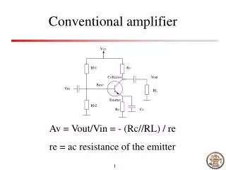
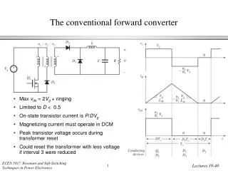
The conventional forward converter. Max v ds = 2 V g + ringing Limited to D < 0.5 On-state transistor current is P / DV g Magnetizing current must operate in DCM Peak transistor voltage occurs during transformer reset

The conventional forward converter
E N D
Presentation Transcript
The conventional forward converter • Max vds = 2Vg + ringing • Limited to D < 0.5 • On-state transistor current is P/DVg • Magnetizing current must operate in DCM • Peak transistor voltage occurs during transformer reset • Could reset the transformer with less voltage if interval 3 were reduced
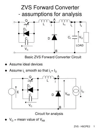
The active-clamp forward converter • Better transistor/transformer utilization • ZVS • Not limited to D < 0.5 Transistors are driven in usual half-bridge manner:
Approximate analysis:ignore resonant transitions, dead times, and resonant elements
Charge balance Vb can be viewed as a flyback converter output. By use of a current-bidirectional switch, there is no DCM, and LM operates in CCM.
Peak transistor voltage Max vds = Vg + Vb = Vg /D’ which is less than the conventional value of 2 Vg when D > 0.5 This can be used to considerable advantage in practical applications where there is a specified range of Vg
Design example • 270 V ≤ Vg ≤ 350 V • max Pload = P = 200 W • Compare designs using conventional 1:1 reset winding and using active clamp circuit
Conventional case Peak vds = 2Vg + ringing = 700 V + ringing Let’s let max D = 0.5 (at Vg = 270 V), which is optimistic Then min D (at Vg = 350 V) is(0.5)(270)/(350) = 0.3857 The on-state transistor current, neglecting ripple, is given by ig = DnI = Did-on with P = 200 W = Vg ig = DVg id-on So id-on = P/DVg = (200W) / (0.5)(270 V) = 1.5 A
Active clamp case:scenario #1 • Suppose we choose the same turns ratio as in the conventional design. Then the converter operates with the same range of duty cycles, and the on-state transistor current is the same. But the transistor voltage is equal to Vg /D’, and is reduced: • At Vg = 270 V: D = 0.5 peak vds = 540 V • At Vg = 350 V: D = 0.3857 peak vds = 570 V • which is considerably less than 700 V
Active clamp case:scenario #2 • Suppose we operate at a higher duty cycle, say, D = 0.5 at Vg = 350 V. Then the transistor voltage is equal to Vg /D’, and is similar to the conventional design under worst-case conditions: • At Vg = 270 V: D = 0.648 peak vds = 767 V • At Vg = 350 V: D = 0.5 peak vds = 700 V • But we can use a lower turns ratio that leads to lower reflected current in Q1: • id-on = P/DVg = (200W) / (0.5)(350 V) = 1.15 A • Conclusion: the active clamp circuit resets the forward converter transformer better. The designer can use this fact to better optimize the converter, by reducing the transistor blocking voltage or on-state current.
Active clamp circuits: some examples Basic switch network reduces to: (if the blocking capacitor is an ac short circuit, then we obtain alternately switching transistors—original MOSFET plus the auxiliary transistor, in parallel. The tank L and C ring only during the resonant transitions)
Example: addition of active clamp circuit to the boost converter The upper transistor, capacitor Cb, and tank inductor are added to the hard-switched PWM boost converter. Semiconductor output capacitances Cds are explicitly included in the basic operation.
Active clamp circuit on the primary sideof the flyback converter
Active clamp to snub the secondary-side diodes of the ZVT phase-shifted full bridge converter