Understanding the Depletion Region in p-n Junctions and Its Effects on Junction Capacitance
60 likes | 187 Views
This text explores the depletion region in p-n junctions, where electrons and holes diffuse across regions, leaving behind fixed ionized charges. These charges generate an electric field that counters diffusion currents, creating a depletion region characterized by a balance between ionized donors and acceptors. The depth of the depletion region varies depending on the doping concentration of materials on each side, forming a capacitor within the junction. This analysis aids in understanding junction capacitance and the physical principles governing semiconductor behavior.

Understanding the Depletion Region in p-n Junctions and Its Effects on Junction Capacitance
E N D
Presentation Transcript
Depletion Region ECE 2204
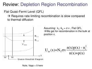
Depletion Region • As electrons diffuse from the n region into the p region and holes diffuse from the p region into the n region, the ionized donors and acceptors that created the electrons and holes are left behind as the donors and acceptors are bound in place by their bonds with the Si atoms in the crystal. • These fixed charges induce an electric field in the semiconductor, which produces a drift currents that counters the diffusion currents. • The depletion region is the distance over which the electric field is induced.
Depletion Region • The number of ionized acceptors in the depletion region is equal to the number of ionized donors. • In the diagram below, the n-type region is more lightly doped (has fewer donors per cubic centimeter) and the p-type region. • Therefore, the depletion width extends deeper into the n-region and the p region. • x = 0 is the metallurgical interface between the p-type material and the n-type material. -xp and xn are the edges of the depletion region in the p-type and n-type material, respectively.
Depletion Region • The depletion region is inversely proportional to the doping concentration of the more lightly doped side of a p-n junction
Junction Capacitance • Any time a depletion region exists, a capacitor is formed. • In the case of the p-n junction • The p region on side of the depletion region and the n side on the other form the parallel plates of the capacitor • The width of the depletion region is the thickness of the insulator between parallel plates.
Junction Capacitance • With no applied voltage • where eris the relative dielectric constant of the semiconductor, eo is the vacuum permittivity, W is the depletion width, and A is the cross-sectional area of the contact between the p and n regions.

