GTK - TDC analysis
GTK - TDC analysis. Lukas Perktold 17 th March 2010. Progress. Layout vs Schematic ► Parasitic extraction Corner Simulation ► Check basic functionally of circuit ? check Loop Dynamics. ERROR identified - TDC runs at 320 MHz. Delay Line – Sakari vs Mine. Delay depends on

GTK - TDC analysis
E N D
Presentation Transcript
GTK - TDC analysis Lukas Perktold 17th March 2010
Progress Layout vs Schematic ► Parasitic extraction • Corner Simulation ► Check basic functionally of circuit ? check Loop Dynamics ERROR identified - TDC runs at 320 MHz
Delay Line – Sakari vs Mine • Delay depends on RFN_min: fixed at 506.9 mV (50 uA) RFN: adjusted by the Loop • difference in delay curve (Sakari vs Mine) • may used different methods? (bias current, measurement) • rather big difference between different corners
TDC – Current Cons. TDC in locked state -> delay = 97 ps • Biasing: 75.8 uA • SEtoDE: 56.9 uA • CP: 622 uA • PD: 80 uA peak: 665 uA • Counters: 537 uA peak: 4 mA • Coarse HRs: 100 uA x2 • PG Bank: off + = 33.6 mA • 65 % of the current consumption due to the “8x buffer” • high peak current for digital parts of TDC
Delay Line – Supply Distribution MQ wire: 350u x 3u R□ = 33.9 mOhm Reff = 2x 4 Ohm Ieff = 33.4 mA Vdrop = 2x 133.6 mV
TDC – Operating Point • TOP level wiring only rough estimate • separated power domains in simulation (several) New Operating Point: VDDD = 1.5 V RCLK_Bias = 250 uA RFN = 588.5 mV (to VDSS) • Different power domains for TDC and Biasing-Current • Loop locks at 320 MHz with new operating point out of Reset
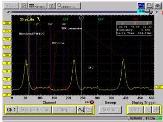
Delay Line - Measurement Thanks to Matthew for the plot RCLK_Bias = 250 uA RFN = 750 mV • simulation and measurements differ (Corners? / inaccurate model?)
Outline • match simulation to measurements • move to new DK version • make a list of all errors found through measurements • check if the all errors can be explained (might have more errors in the design) - Weak performance (e.g. INL) of the TDC for rising edges - Zero dies out for higher frequencies - compare RFN settling values - ... • propose solution to errors found and document them