Download
1 / 10
110 likes | 130 Views
Explore the History and Evolution of Chip Design at PSI from 1989 to 2007, with the inception of a New Chip Design Core Group in 2008. Learn about the advanced tech functions and experiments conducted at PSI, including significant developments like the SAC silicon strips, signal samplers, and various chip prototypes such as APC128 and Domi Sampling Chip. Discover the collaboration model with internal PSI groups and external university partners, fostering a dynamic environment for cutting-edge chip design projects. Join us on this transformative journey of chip innovation at PSI.

E N D
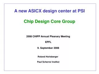
A new ASICX design center at PSI Chip Design Core Group 2008 CHIPP Annual Pleanary Meeting EPFL 9. September 2008 Roland Horisberger Paul Scherrer Institut
History of Chip Design at PSI (1989 2007) • Chip design at PSI started in 1989 for planned B-Meson factory at PSI • Tech.FunctionExperiment • PSI 1 SAC 3m Silicon strip readout 32 channels mnexperiment • PSI 2 SAC 3m Signal sampler (drift chamber), 300 MHz PiBeta exp. • PSI 18 SAC 1m Silicon strip pipeline(32) chip APC128 H1-vertex detector • HERMES (MSGC) • PSI 26 DMILL Pixel Prototype Chip for CMS • PSI 30 DMILL Pixel Testbeam Chip for CMS • PSI43 DMILL Full CMS Pixel ROC • PSI 46 0.25m Full CMS Pixel ROC ( final chip) CMS Pixel ROC • PSI ~65 Chips for x-ray Pixel Systems, x-ray Strips, Signal Samples • PILATUS 1,2 & XFSMYTHEN DRS MEG, Magic
Chip Design at PSI (1989 2007) PSI SLS X-ray Pixel PILATUS chips (Ch. Brönnimann) PSI SLS X-ray Strips MYTHEN chips (B. Schmidt) PiBeta Experiment wave form sampler Chip (R.Schnyder) ASIC CAD installation by PSI LTP-group (R.H.) Desy Zeuthen silicon strip readout rad. hard APC128 chips (I. Tsurin) MEG Experiment wave form sampler DRS chips (St.Ritt) Past working model: Other groups plug into existing ASIC CAD installation & culture with their own manpower and get quickly productive good for us too ! maintained critical size of effort !
New Chip Design Core Group 2008 • New Chip Design Core Team maintains ASIC CAD • PSI internal groups and external University groups as plug in users • Chip Design Core Team helps, but does not their work ! New model: PSI SLS Pixel Group New x-ray pixel det. PILATUS XFS PSI CMS Pixel Group SLHC upgrade New Pixel ROC PSI Group PSI experiment Chip to be done ASIC CAD installation by PSI Chip Design Core Team University Groups e.g. LHCb upgrade new super chip
Chip–Design–Core–Group at PSI (Since 2008) • Over last 10 years very good experience inside PSI with following model: • A core group keeps basic chip design CAD effort going and works on own projects (chips) (historical done by CMS pixel group) • Interested groups can plug in and get helped with basic start up, support, consultation and evtl. cooperation • Examples: Pilatus x-ray pixel detector for SLS • Mythen Silicon Strip x-ray detector for SLS • APC128_DSM ( DESY, Zeuthen) • Domino Sampling Chip for MEG, Magic, etc. With new created Chip-Design-Core-Group model is now official. Expand “plug in user groups” beyond PSI to CH university groups • PSI acts as CH facility for activities with major setup efforts ( CAD maintenance) • Strengthens links PSI Universities
Chip–Design–Core–Group at PSI Currently 3 people in PSI Electronic group of Nick Schlumpf (LTP): Beat Meier Physicist / Electric Engineer Roberto Dinapoli Electric Engineer Xintiab Shi Electric Engineer
The MythenII readout chip • x-ray photon silicon strip readout. • 128 channels , 50 um pitch • 24 bit counter/strip -> high dynamic range • Low noise -> 195 ENC, high rate 1MHz MythenII Strip sensor
CMS Pixel Read Out Chip IBM_PSI46 • 0.25mm CMOS Technology • 1.28 million transistors • radiation hard design ( ~40Mrad) 9.8 mm CAD picture of a pixel 100m 150m • 251 Transistors /pixel
0.2-2 ns Inverter “Domino” ring chain IN Waveform stored Out FADC 33 MHz Clock Shift Register (Stefan Ritt. PSI) Domino Ring Sampler (DRS) Chip • 12 channels each 1024 samples deep • Sampling speed 10 MHz … 5 GHz • 0.25 mm CMOS process 5 x 5 mm2, radiation hard