Download
1 / 29
290 likes | 434 Views
Development of High Data Readout Rate Pixel Module and Detector Hybridization at Fermilab. S.Zimmermann, S.Kwan, G.Cancelo, G.Cardoso, S.Cihangir, D.Christian, R.Downing, J.Hoff, A.Mekkaoui, A.Vargas Trevino * , R.Yarema Fermi National Accelerator Laboratory (USA)

E N D
Development of High Data Readout Rate Pixel Module and Detector Hybridization at Fermilab S.Zimmermann, S.Kwan, G.Cancelo, G.Cardoso, S.Cihangir, D.Christian, R.Downing, J.Hoff, A.Mekkaoui, A.Vargas Trevino*, R.Yarema Fermi National Accelerator Laboratory (USA) *Universidad Automona de Puebla (Mexico) PIXEL 2000 Genoa, June 5-8, 2000
Outline • Introduction • Proposed Pixel Detector MCM • Constraint: data rate • Block diagram and MCM • Data readout variation • Characteristics of the flex circuit technology • Prototype and experimental results • Hybridization studies • Vendor search • Indium bumps • Solder bumps • Conclusions Development of High Data Readout Rate Pixel Module and Detector Hybridization at Fermilab
Introduction: BTeV Pixel Detector • Pixel half plane: approximately 510 cm. • 868 pixel modules • Position: 6 mm from the beam. • “Shingle” approach allows for 100% coverage in a single plane side. Development of High Data Readout Rate Pixel Module and Detector Hybridization at Fermilab
Constraint: Data Rate • The Pixel detector will be used for the lowest level trigger all pixel hit data needs to be readout • Simulation: assume • Luminosity of 21032 cm2s1 ( an average of two interactions per crossing) • Threshold: 2000 e– • Magnetic field: 1.6 T • Does not use the angle required for “shingling” • Chip data rate depends on: • Chip active area • Distance from the beam • Number of pulse height ADC bits; assume 3 bits • The way the data is arranged, etc. Development of High Data Readout Rate Pixel Module and Detector Hybridization at Fermilab
Constraint: Data Rate • Example: Column with more hits Beam Chip with more hits Development of High Data Readout Rate Pixel Module and Detector Hybridization at Fermilab
Block diagram and MCM • Readout through the Serializer chip. • Serializer input: 17 bits at 60 MHz. • Two 12 bits readout busses. • One 6 bits readout bus. • Remaining bits used to readout control. • Safety margin: range from 3.1 to 4.6 from average data rate of this example. Development of High Data Readout Rate Pixel Module and Detector Hybridization at Fermilab
Block diagram and MCM • PIXEL MODULE • “Sandwich” of flex cable, pixel sensor and readout chips. • Control and readout through fiber optics. Development of High Data Readout Rate Pixel Module and Detector Hybridization at Fermilab
Multi-Chip Module • VCSEL and Pin diode assemblies Methode Electronics, Inc. Development of High Data Readout Rate Pixel Module and Detector Hybridization at Fermilab
Data Readout Variation • This proposed solution has some drawbacks: • Requires the design of one more integrated circuit • The area for the three chips and connectors is significant • To assemble the modules we need all three rad-hard chips • A variation is differential readout: • Use differential copper wires for a point-to-point connection to the side of the beam pipe. • The radiation in this area is 10 Krads (hopefully) allowing the use of commercial parts. • From the side, fiber optics readout. • Preliminary studies show that the mass of the copper cables (power and data/control transmission) would increase by less than 15%. Development of High Data Readout Rate Pixel Module and Detector Hybridization at Fermilab
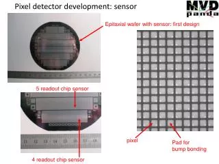
LAYER PAIR Cu / Ni / Au L aye r P a ir 1 D i e l ec tri c Laser Thru-Hole L aye r pa ir 2 Condu c to r Characteristics of the Flex Circuit Technology Fujitsu Computer Packaging Technologies, Inc. (FCPT) • Four layers is standard, six layers is doable. • Dielectric base film: Upilex or Kapton. Development of High Data Readout Rate Pixel Module and Detector Hybridization at Fermilab
Characteristics of the Flex Circuit Technology • Line width: standard, 20 m • Line to line clearance: standard, 20 m • Line thickness: standard, 5 m Development of High Data Readout Rate Pixel Module and Detector Hybridization at Fermilab
Characteristics of the Flex Circuit Technology • Z Via • Via cover pad diameter: 108 m • Through via hole diameter: 35 m top, 18 m bottom • Via center spacing: 208 m Development of High Data Readout Rate Pixel Module and Detector Hybridization at Fermilab
Prototype and Experimental Results Five FPIX1’s bonded to a FCPT flex circuit Development of High Data Readout Rate Pixel Module and Detector Hybridization at Fermilab
Prototype and Experimental Results • Test stand based on standard instrumentation. • PC running LabView • Control by GPIB • Readout by Ethernet Development of High Data Readout Rate Pixel Module and Detector Hybridization at Fermilab
Prototype and Experimental Results• Data Transmission • Parameters of transmission lines • Simulation : PSpice Five FPIX1’s bonded to a FCPT flex circuit Development of High Data Readout Rate Pixel Module and Detector Hybridization at Fermilab
Prototype and Experimental Results• Data Transmission (Simulation) Development of High Data Readout Rate Pixel Module and Detector Hybridization at Fermilab
Prototype and Experimental Results• Development of High Data Readout Rate Pixel Module and Detector Hybridization at Fermilab
Prototype and Experimental Results Performance of five FPIX1’s bonded (no sensor) to a FCPT flex circuit Development of High Data Readout Rate Pixel Module and Detector Hybridization at Fermilab
First Prototype and Experimental Results• • Hybridized sensor assembled on the prototype board Development of High Data Readout Rate Pixel Module and Detector Hybridization at Fermilab
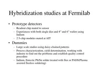
Hybridization Studies • Prototype detectors • Readout chip mated to sensor • Experiences with both single dies and 4” and 6” wafers using Indium • 2 5-chip modules mated at AIT • Dummies • Large scale studies using daisy-chained patterns • Process characterization, yield determination, working with industry to find out the problems and establish quality control procedure • Indium, Eutectic Pb/Sn solder treated with flux or PADS(Plasma assisted fluxless soldering) Development of High Data Readout Rate Pixel Module and Detector Hybridization at Fermilab
Vendor search • A lot of enquiries/contacts but most companies are not interested or consider the job too challenging • Prototyping – BOEING, AIT (both used indium and could do wafer or single dies) • Dummies • AIT (indium at 30 mm pitch) • AIT also tested wafer bumping with 200 mm thick wafers • MCNC/Unitive (solder both flux and fluxless); only 6” wafers (needs modification for 4”). Development of High Data Readout Rate Pixel Module and Detector Hybridization at Fermilab
Indium Bumps • • Indium bumps on readout chip done at AIT Development of High Data Readout Rate Pixel Module and Detector Hybridization at Fermilab
Indium Bumps Results on Indium-bumped (AIT) prototype detectors: Hit-map for three FPIX1-implemented detectors using radioactive source Development of High Data Readout Rate Pixel Module and Detector Hybridization at Fermilab
Solder Bumps • Tests on dummies from MCNC/Unitive • Structures with 50 mm pitch (BTeV) and 150 mm pitch(CMS) on same wafer • 80 PADS single-chip assemblies and 38 fluxed single-chip assemblies (BTeV) • US-CMS also tested 5 double-chip assemblies and 1 5-chip assembly (using flux-less solder) • Check connectivity between matched pair of pads using a semi-automatic probe station • Sometimes, need to apply a low voltage to break through • Also look for shorts between neighbors Development of High Data Readout Rate Pixel Module and Detector Hybridization at Fermilab
Solder Bumps • Results on connectivity • Much better results in the PADS assemblies than the ones using flux. The latter ones have a lot of visible residues • Concentrate only on PADS assemblies • 6 out of 71 assemblies (size of a 7.2 8 mm chip) have a lot of opens due to operator error. Assembly yield is 65/71 or 91.5% • 190 traces per assembly. 52 opens. Trace yield =99.58% • 26 bonds per trace. Bump yield =99.98% • Preliminary results from CMS module assemblies are comparable. Development of High Data Readout Rate Pixel Module and Detector Hybridization at Fermilab
Solder Bumps • • Problems • Operator error – gross misalignment by one column • Channels need voltage to break through –thought to be due to incomplete removal of oxide on Al before UBM was put on • Bridges (see X ray picture) • Irregular reflow • Lab vs cleanroom condition • Module assembly –PADS process needs modification Development of High Data Readout Rate Pixel Module and Detector Hybridization at Fermilab
Solder Bumps • Defect joint Development of High Data Readout Rate Pixel Module and Detector Hybridization at Fermilab
Conclusions: MCM • Option for data readout needs to be studied in details. • The prototype of the Pixel module with the sandwich of readout chip, detector, and circuit interconnect must be assembled and characterized. • Good agreement between circuit simulation and real measurements. • The present prototype shows good performance characteristics. Development of High Data Readout Rate Pixel Module and Detector Hybridization at Fermilab
Conclusions: Bump Bonds • Satisfactory results on real detectors using Indium • Dummy tests on 30mm ongoing • Fluxless solder by MCNC has good bond yield • Whole chip losses need to be better understood and controlled • Module assembly – non-industrial standard (closely abutted to one another); MCNC needs to learn how to do this • Next round – real detectors will be bumped and bonded at MCNC Development of High Data Readout Rate Pixel Module and Detector Hybridization at Fermilab