1 / 1

FPGA-Based Interface Design with SPI Flash and SDRAM for ADSP-BF538F Microprocessor

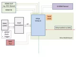
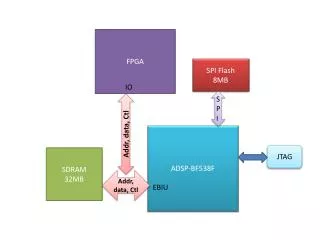
This design utilizes an FPGA to interface with an 8MB SPI Flash memory and a 32MB SDRAM for the ADSP-BF538F microprocessor. The system architecture includes dedicated control, address, and data lines for both memory types, ensuring efficient data handling and storage. The FPGA acts as the intermediary, facilitating communication between the microprocessor and memory components via JTAG for configuration and debugging. This setup enhances the performance of embedded systems requiring significant memory resources and fast data access.

Download Presentation

FPGA-Based Interface Design with SPI Flash and SDRAM for ADSP-BF538F Microprocessor

An Image/Link below is provided (as is) to download presentation Download Policy: Content on the Website is provided to you AS IS for your information and personal use and may not be sold / licensed / shared on other websites without getting consent from its author. Content is provided to you AS IS for your information and personal use only. Download presentation by click this link. While downloading, if for some reason you are not able to download a presentation, the publisher may have deleted the file from their server. During download, if you can't get a presentation, the file might be deleted by the publisher.

E N D

Presentation Transcript


  1. FPGA SPI Flash 8MB IO SPI Addr, data, Ctl ADSP-BF538F JTAG SDRAM 32MB Addr, data, Ctl EBIU

More Related