FPGA CAD
FPGA CAD. 10-MAR-2003. Content. FPGA CAD design flow; Placement; Routing. (top ten hottest VLSI CAD problems). FPGA Design Flow. Designing with FPGAs is much like the ASICs technology.

FPGA CAD
E N D
Presentation Transcript
FPGA CAD 10-MAR-2003
Content • FPGA CAD design flow; • Placement; • Routing. • (top ten hottest VLSI CAD problems)
FPGA Design Flow • Designing with FPGAs is much like the ASICs technology. • The Computer Aided Design (CAD) software provided by the FPGA vendor or third part is used to convert the given digital circuit (schematic or a high level description in VHDL or Verilog) into a stream of bits, which is then used to download to the FPGA.
CAD Tools Max+Plus
A Typical FPGA CAD Flow Design Entry Synthesis Logic Optimization Placement Packing LUTs to CLBs Mapping to k-LUT Routing Simulation Download to FPGA
Problem define • Assign position(X, Y) to modules; • Placement to minimize: • total wirelength; • critical path wirelength; • a combination of them. • Estimated model: • Circuit quality is determined by placement + routing; • Routing is a NP-hard problem. • NP-hard problem. (n!) • Time is a big issue. • Quality and time tradeoff.
Heuristic method • Constructive methods: • Partitioning method: min-cut; • Clustering. • Iterative improvement: • Begin with a random or constructive placement; • Iterate to improve it; • Force directed method; • Simulated annealing. • Other method: • Genetic algorithm;
Min-Cut Minimize cuts during partition
Force directed method • Classical mechanics; • Using Hooke’s law; • Force vector computed on each module corresponding to all nets connections; • Solve a set of non-linear differential equations. force
Simulated annealing • Generates best results; (industry standard) • Run time is a issue. • Model a physical annealing process. • VPR placer (placement tools available to us, developed in UoT).
Physical Annealing • Take a metal and heat to high temperature until liquidized; • Allow it to cool slowly, metal is annealed to a low temperature; • Atoms in the metal are at transfer from high energy states to low energy states; • Can accept “bad” moves to get global minima. • Avoid getting trapped in local minima.
Routing-Find the path • Maze routing; • Pathfinder.
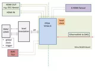
Routing Resource Connection Block Switch Block
Pathfinder router • Based on maze router; • Shows very high quality results; • Negotiation-based router; • Each net negotiates the use of shared resources with other nets until none of the resources are shared; • Extra weights are added to shared resources. • VPR router;
Design Entry • The description of a logic circuit can be entered by using a schematic capture program; • VHDL and Verilog interpreter.
Synthesis • A circuit description such as VHDL, is first converted to a netlist of basic gates. This process called synthesis.
Logic Optimization • technology independent; • Improve circuit, while keep functionality correct;
Mapping to LUTs • The gates then are mapped into k-input lookup tables (LUT). (most basic brick of FPGA) • Chortle. (available to academic, developed in UoT)
Packing LUTs into CLBs • Configurable Logic Block (CLB); • Grouping the LUTs into CLBs; • Simi liar to circuit clustering. • Vpack. (available to academic, developed in UoT)
Placement • Placement is to determining the physical location of each CLBs on the FPGA;
Routing • Realize connections among the CLBs by selecting routing resource. • wire segments and; • routing switches.
Simulation • After placement and routing, the implemented design is simulated to ensure its functioning and to verify the timing issues. • Design errors can be found and corrected at this stage.
Download bits file to FPGA • Once all the necessary steps are completed for implementing the design, the CAD system can download the result to the programming unit that is used to configure the FPGA; • After this stage, the programmable device is configured and ready for use.