Download
1 / 23
230 likes | 336 Views
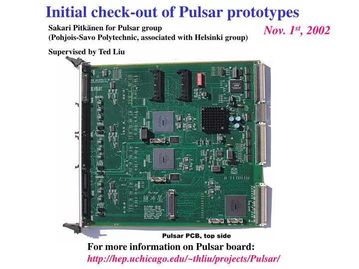
Initial check-out of Pulsar prototypes. Sakari Pitkänen for Pulsar group (Pohjois-Savo Polytechnic, associated with Helsinki group) Supervised by Ted Liu. Nov. 1 st , 2002. For more information on Pulsar board: http://hep.uchicago.edu/~thliu/projects/Pulsar/. Goal for the initial check-out.

E N D
Initial check-out of Pulsar prototypes Sakari Pitkänen for Pulsar group(Pohjois-Savo Polytechnic, associated with Helsinki group) Supervised by Ted Liu Nov. 1st, 2002 For more information on Pulsar board: http://hep.uchicago.edu/~thliu/projects/Pulsar/
Goal for the initial check-out • Test all the interfaces, including spare lines • Prepare firmware and software to come up with an automatic test program for board check out later SRAMs Gigabit Ethernet RF clock Pulsar is designed to be fully self-testable
Six weeks of prototype testing • First prototypes received on Sept. 19th 2002 • Week One • VME access to all three FPGAs • Data merging and SLINK formatting • Week Two • SVT data path: input and output • SLINK data to AUX card • VME access to SRAMs • Week Three • Recorded data into PC via SLINK to PCI interface, with input data from SLINK test tools • Week Four • L1 data path: input and output • Finalized Hotlink mezzanine cards Rev. B design, simulated with motherboard
Six weeks of prototype testing • Week Five • Data formatting up to 100 MHz clock • RF clock input connection • Rev. B Hotlink mezzanine cards received Oct. 25th • Week Six • Rev. B Hotlink mezzanine cards (Tx and Rx) work with Pulsar motherboardOct 28th • Hotlink Bit-Error-Rate with Hotlink evaluation board (run for 40 hours so far) • Recorded data into PC via SLINK to Gigabit Ethernet interface • TSI interface connection • 25 spare lines (P3) • Pulsar inter-communcation lines (P2) • CDF control signals • Finished initial check-out on Oct. 30th 2002
Two Pulsar prototypes received Sept. 19th, 2002
Initial VME access to all three FPGAs Sept. 21st, 2002 VME chip • Read only register • Read / write register • LEDs • Internal RAM • Test pulse • VME access to all FPGAs works 3 LEDs DataIO FPGA 1 RAM Registers 3 LEDs Test pulse DataIO FPGA 2 RAM Registers Test pulse Control FPGA 3 LEDs RAM Registers Test pulse
SLINK formatting Sept. 26th, 2002 • Input data is uploaded to both DataIO FPGAs • DataIO FPGAs send merged input data in SLINK format to Control FPGA • Control FPGA merges incoming data and sends it out in SLINK format from P3 • Outgoing data is stored into a Spy FIFO in each FPGA, and it can be read from the FIFOs using VME • Data in the Control FPGA Spy FIFO matches the data uploaded to input RAMs VME chip DataIO FPGA 1 Input RAMs Spy FIFO DataIO FPGA 2 Input RAMs Spy FIFO P3 Control FPGA Spy FIFO
SLINK formatting Sept. 27th, 2002 • Outgoing SLINK data goes from P3 to AUX card, which has a SLINK SLIDAD on it • Outgoing data was checked with logic analyser from SLIDADs debug pins • Data seen in the SLIDAD matches the data uploaded to input RAMs AUX card SLIDAD
SVT data path Oct. 1st, 2002 • Input data is uploaded to Control FPGA RAM using VME • Control FPGA sends SVT data out from SVT output • All FPGAs receive incoming SVT data • Data is read from each FPGA using VME • Sent SVT data and received SVT data match VME chip DataIO FPGA 1 Receiver FIFO DataIO FPGA 2 SVT data in Receiver FIFO SVT data in Control FPGA SVT data in SVT cable Receiver FIFO SVT data out RAM
Initial VME access to SRAMs Oct 4th, 2002 • Two 128Kx36 SRAMs on board • Each DataIO FPGA has control of one SRAM • Wrote and read SRAMs through VME • Loaded SRAMs with 128K test patterns • Repeated test • Sent and received data matched every time VME chip DataIO FPGA 1 SRAM DataIO FPGA 2 SRAM
Recorded SLINK data into PC Oct 7th, 2002 • Incoming data is created with the SLINK test tools • Data comes in to Pulsar board from SLINK RX mezzanine cards • Tested data formatting up to 100 MHz clock on Pulsar board AUX card SLINK RX mezzanine card SLINK RX mezzanine card Clock SLINK test tools P3 SLINK LSC
Recorded SLINK data into PC Oct 7th, 2002 • Data goes out from P3 to AUX card • Data was received by SLINK LSC and sent to PC • Data was recorded and checked with Linux PC AUX card SLINK RX mezzanine card SLINK RX mezzanine card SLINK LDC Tested with internal clock up to 100 MHz Oct. 21 P3 SLINK LSC
L1 data path: input and output Oct 17th, 2002 • Data is sent out from one Pulsar and received by another one VME DataIO FPGA 1 Input register • Control FPGA sends data from internal RAM DataIO FPGA 2 Input register Control FPGA VME Input register • Data is received by all three FPGAs • Read-out through VME • Data matches Control FPGA OutputRAM
Pulsar with Rev B Hotlink mezzanine cards Oct. 28th 2002 (received on Oct. 25th) • Data is driven out by L1As Hotlink TX Hotlink TX Hotlink RX Hotlink RX • Tested with 20Mhz as well as CDFCLK x 4 • Data matches
Rev B Hotlink Bit-Error-Rate test Oct. 29th 2002 • Using BIST (built-in-self-test) mode • Up to 40 hours so far, zero error count Hotlink TX Hotlink evaluation board
Recorded SLINK data into PC with Gigabit Ethernet interface Oct 29th, 2002 • Using SLINK to Gigabit LSC from ANL (Bob Blair and John Dawson) AUX card Netgear GA621 SLINK LSC Tested with internal clock up to 100 MHz Oct. 21 ANL LSC NetGear GA621 SLINK LSC • Two options to record data: Gigabit Ethernet or SLINK to PCI interface
TSI interface connection Oct 29th, 2002 VME chip • Data sent and received by Control FPGA • Data matches TS cable Control FPGA In/out Registers Thanks Stephen Miller who made the cable for us
Pulsar P3 spare lines Oct 29th, 2002 VME chip • Pulsar has 25 spare lines to P3 • Data sent from Control FPGA • Checked with Logic Analyzer from P3 backplane • Data matches P3 Control FPGA LA Output register
Tested Pulsar P2 inter-communication lines Oct 29th, 2002 VME chip • Pulsar has five SVT style inter-communication lines on P2 • Data is sent from Control FPGA on one Pulsar and received by all three FPGAs on the other one • Data matches DataIO FPGA 1 Input register P2 DataIO FPGA 2 Input register Control FPGA In/out registers
P2 CDF control signals Oct 30th, 2002 • Pulsar FPGAs see ALL P2 CDF control signals • Used Testclk to toggle all signals • Signals recorded by circular buffer RAM in each FPGA • Also checked with Logic Analyzer • Data matches VME chip DataIO FPGA 1 RAM DataIO FPGA 2 RAM Control FPGA RAM
L2 teststand Thanks Cheng-Ju and Arnd who helped us to setup test crate intially
Summary • Initial check-out finished, tested all interfaces including spare lines • Most tests were done using Pulsar self-test capability • So far, no single problem found with Pulsar design Future • Short term (next two month) • Fine tune firmware and software to automate testing procedures • Test for robustness! • Document all the details • Load two more Pulsar boards • Send out Taxi mezzanine cards • Longer term (early next year) • Develope firmware and software for teststand, for each data path • Test with real L2 data path • Two Pulsar boards will be dedicated for firmware development, • While the other two will be dedicated for teststand
Summary spare SRAMs RF clock Gigabit Ethernet • Taxi mezzanine cards are at layout stage • Interface to Taxi mezzanine cards is the same as for Hotlink mezzanine cards