Lab 6 : Digital Display Decoder :
80 likes | 294 Views
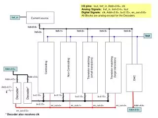
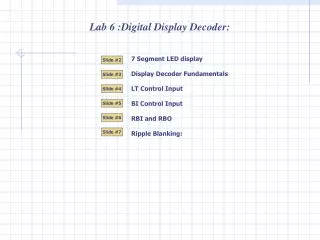
Lab 6 : Digital Display Decoder :. 7 Segment LED display. Slide #2. Display Decoder Fundamentals. Slide #3. LT Control Input. Slide #4. BI Control Input. Slide #5. RBI and RBO. Slide #6. Slide #7. Ripple Blanking:. a. a. 1. 1. b. b. 0. f. f. 0. Common Catthode. 0. 0. g.

Lab 6 : Digital Display Decoder :
E N D
Presentation Transcript
Lab 6 :Digital Display Decoder: 7 Segment LED display Slide #2 Display Decoder Fundamentals Slide #3 LT Control Input Slide #4 BI Control Input Slide #5 RBI and RBO Slide #6 Slide #7 Ripple Blanking:
a a 1 1 b b 0 f f 0 Common Catthode 0 0 g g 1 5V 1 c c 0 Common Anode e e 1 0 0 d d 1 1 Lab 6 : 7 Segment LED display Digital displays come in various packages and arrangements. The 7 Segment LED display (7 seg disp) is one of the most common and has been around for many years. The display is an IC with 7 LED’s. Lighting up combinations of LED’s can display any number. The 7 LED’s are labeled with industry standard identifiers (a, b, … g). The identifiers are used to designate the position of each LED. There are 2 types of display packages. The package shown is called Common Cathode.It lights the LED when a logic 1 is applied to the input segment. The common pin must be connected to ground. Here is how the number 7 is displayed… The other package is called Common Anode.It lights the LED when a logic 0 is applied to the input segment. The common pin must be connected to Vcc. Here is how the number 7 is displayed… Slide #2
a b f a 1 A 1 5 b 0 B 0 g f 1 c C 1 e Common Cathode D g 1 0 5V c 1 d LT e 0 RBI d 1 BI RBO Decoder Lab 6 : 7 Segment Decoder The 7 Segment LED display package is connected to a decoder. The decoder receives the binary code at inputs D C B A and lights the appropriate segments. This display decoder has active high outputs. It connects to a Common Cathode display. The decoder has 3 Active Low control inputs LT, RBI, BI. They will be disabled for now and explained later. The decoder has an internal logic gate system that takes the 4 bit number applied to D C B A and lights up the LEDs to display that number. Here is an example of the decoder displaying the number 5. The number 5 is applied to the input. D is MSB and A is LSB. The decoder internal logic gate system outputs the binary combination to display 5 at a, b, … g. Logic 1 at an output forward biases the LED and it lights it up. Logic 0 produces no LED current. Slide #3
a b f 1 1 0 a 0 D 1 5 0 1 b 5 1 g C 1 1 c f 0 Common Cathode 0 B 5v e 1 5v 1 1 1 A g 1 1 d 1 c 0 LT e 5V 5V RBI 1 1 d RBO BI Decoder Lab 6 : LT Control Input : The decoder has 3 control inputs: LT, RBI, BI. It also has one control output: RBO. The control I/O can be used to implement various functions or they can be disabled. This section describes the Lamp Test (LT) feature. LT : is the Lamp Test input. It is active LOW. It can be connected to a switch (or control system). The user can flip the switch to test all the segments of the LED display. When the switch is in the 5 V position it disables the LT feature. DCBA (#5) controls the display. When the switch is in the 0 V position it enables the LT feature. All segments light. LT overrides the conditions at DCBA (#5). The user can now check the display for burned out segments. Slide #4
0 0 0 1 5 0 0 0 1 0 5V 0 5v 0 a 1 0 b 0 1 5 f 1 a 0 D 1 b 1 g C c f Common Cathode B 1 5V e 0 5v A g 1 5 d c LT e RBI d RBO BI Decoder Lab 6 : BI Control Input : The decoder BI input is the Blanking Input. This section describes the BI feature. BI : is the Blanking Input. It is active LOW. It can be connected to a switch (or control system). The user can flip the switch to turn off all the segments of the LED display (blank the display). When the switch is in the 5 V position it disables the BI feature. DCBA (#5) controls the display. When the switch is in the 0 V position it enables the BI feature. All segments turn off. BI overrides the conditions at DCBA (#5). Slide #5
a 0 0 1 0 0 0 b 0 0 1 0 0 0 f 1 a 0 0 D 0 b 0 5v 0 g C 0 5V c f 5v 0 Common Cathode B 1 5V e 1 A g 0 1 d c LT e RBI 0 1 d RBO BI 0 indicates “zero” is being blanked 1 Indicates 0 is displayed Decoder Lab 6 : RBI and RBO Control : The RBO output is the RippleBlankingOutput. It works with RBI (Ripple Blanking Input) to blank the number 0. RBI can be connected to a switch (or control system). The user can flip the switch to turn off all the segments of the LED display (blank the display) when the number 0 is input to DCBA. All other numbers 1 … 9 are displayed normally. When the switch is in the 0 V position it enables the RBI feature. RBI blanks the display for the number “0”. The RBO pin (active low) outputs a logic 0 to signal that the display is blank. When the switch is in the 5 V position it disables the RBI feature. DCBA (#0) controls the display. The number “0” is displayed and the RBO pin outputs a logic 1. Why is this feature useful? Because it allows a user to blank leading “0’s” when many displays are link together to make up multiple digit numbers. This feature is described next. Slide #6
Blank Blank 0 0 1 a b c d e f g a b c d e f g a b c d e f g a b c d e f g 5V a b c d e f g 1 1 RBI RBO RBI RBO RBI RBO RBI RBO RBI RBO D C B A D C B A D C B A D C B A D C B A 0 0 0 0 0 0 0 0 0 0 1 1 0 0 0 0 0 1 1 1 Lab 6 : Multiple Digit Ripple Blanking Control : A multiple digit display is aesthetically more appealing to look at if leading “0’s” are blanked. A five digit display looks better if it shows the number 307 than it would if it showed it as 00307. The RBI and RBO control pins allow a user to blank leading “0’s”. The number 00307 is applied to the DCBA inputs of the display decoders. The MSD blanks the zero because RBI=0. It also outputs a zero to RBO to signal display is blank. The next MSD blanks the zero because RBI=0. It also outputs a zero to RBO. The next MSD displays the number 3 because any non-zero number is displayed. It also outputs a one to RBO to signal the display is NOT blank. The next MSD displays the number 0. It also outputs a one to RBO. The LSD always displays it’s number because RBI is always logic 1 (connected directly to 5V). Slide #7