Download

1 / 51
650 likes | 1.32k Views
Module 9 . AVR ATMega32 Elementary Input / Output. ATMega32 Input / Output. One of the basic and essential features designed in a computer system is its ability to exchange data with other external devices, and to allow the user to interact with the system: Input Devices include:

E N D
Module 9 AVR ATMega32 Elementary Input / Output
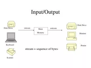
ATMega32 Input / Output • One of the basic and essential features designed in a computer system is its ability to exchange data with other external devices, and to allow the user to interact with the system: • Input Devices include: • Switches, Keyboards, Mice, Scanners, Cameras, etc. • Output devices include: • Lamp/LED/LCD displays, Video monitors, Speakers, Printers, etc. • One or more interface circuits usually are used between I/O devices and the CPU to: • Handle transfer of data between CPU and I/O interface. • Handle transfer of data between I/O device and interface. • Enable the CPU to request the status of data sent/received by the interface. • Common I/O interfaces: • Elementary I/O: Simple two-state devices such as LED and switches • Parallel I/O: Date exchanged one byte at a time. • Serial I/O: Data exchanged one bit at a time. 20112012-I
Microprocessor I/O Interfacing • Most I/O requests are made by applications or the operating system, and involve moving data between a peripheral device and main memory. • There are three main ways that programs communicate with devices. • I/O Addressing • Direct Access Memory • Interrupts 20102011-I
Microprocessor I/O Interfacing • Port-Based (Standard I/O-Direct I/O) • I/O addresses are seperated from memory addresses • Processor’s software reads and writes a port just like a register • E.g., PA0 = 0xFF • Advantages: Do not take memory addressing space • Disadvatage: Use only IN or OUT instrcutions to transfer data • Memory-Mapped I/O • I/O ports treated as memory locations • Advantages: Accessing I/O ports is like accessing memory loactions • Disadvantages: Take memory addressing space 20112012-I
ATMega32 I/O Ports The pins marked ‘Gnd’ are to be grounded, ‘Vcc & AVcc’ are to be given 5V. The Resetpin is also high but we usually prefer to put a switch at this point for the reset of the chips. If the switch is pressed for a minimum pulse of time then it will Resetthe chip. Note: ‘AVcc’ should be connected to 5V supply through a capacitor when using PORTA pins as ADC, though in simple applications capacitor is not necessary. 20112012-I
ATMega32 I/O Port Registers There are three registers associated with Input/ Output Ports in AVR. 20112012-I
ATMega32 I/O Port Registers • Selecting the direction of pin:- • DDRxnbit (in the DDRx Register) selects the direction of this pin. • DDRxn=1, Portx nth pin is configured as an output pin (since there are eight pins in all in a particular port so ‘n’ can be any number between 0-7). • DDRxn=0, Portx nth is configured as an input pin. • Activating the pull resistors:- • PORTxn= 1, the pull up resistors are activated (while the nth pin is configured as input pin) • PORTxn= 0, the pull up resistors are deactivated (for nth pin). • Inputs of the AVR are generally in Hi-Z state. This makes them prone to catching noise and picking up false signals. So it is advisable to activate the pull up resistor to reduce noise 20112012-I
ATMega32 I/O Port Registers • Status of pin when configured as an output pin:- • PORTxn= 1, portx nth pin is driven high (one) • PORTxn= 0, portxnth pin is driven low (zero) • PINxRegister:- • To put it bluntly, the PINx register contains the status of all the pins in that port. • If the pin is an input pin, then its corresponding bit will mimic the logic level given to it. • If it is an output pin, its bit will contain the data that has been previously output on that pin. (The value of an output pin is latched to PINxn bit, you can observe it when we do step by step execution in AVR-Studio shown below) 20112012-I
ATMega32 I/O Pull UP/DOWN Resistors • Pull up resistors are used to pull logic signals up (to logic 1). So when some input signal needs to be set to logic 1, but might need to be changed for some reason to 0 at some other time, a pull-up resistor can keep the signal at logic 1 until the signal is pulled down by something. Typical application for pull up resistors is to connect 4.7 k-ohm (or some other suitable resistor value usually between 1 k-ohm and 10 k-ohm) from the circuit operating voltage (+5V usually) to the input pin. This resistor keep the signal at logic 1. When the signal needs to be set to 0 it is pulled down by connecting that input pin to ground (usually through a button, DIP switch or open collector output of some other part of circuit). • Pull-down resistors work in the opposite way. They keep signal a logic 0 until something connect to signal input to +5V (or whatever the operating voltage of the logic circuit is). 20112012-I
ATMega32 I/O Pull UP Resistor 20112012-I
ATMega32 I/O Port: Example 1 The AVR assembly code below shows how to configure the pins on portA of an AVR ATMega32 microcontroller. .include "m32def.inc" LDI R16, 0xFF ; Load 0b11111111 in R16 OUT DDRA, R16 ; Configure PortA as an Output port LDI R16, 0x00 ; Load 0b00000000 in R16 OUT DDRB, R16 ; Configure PortB as an Input port LDI R16, 0xF0 ; Load 0b11110000 in R16 OUT DDRC, R16 ; Configure first four pins on PortC ; as input and the others as output 20112012-I
ATMega32 I/O Port: Example 2 • The following code will toggle all 8 bits of Port B forever with some time delay between “on” and “off” states: LDIR16,0xFF;R16 = 0xFF = 0b11111111 OUTDDRB,R16;make Port B an output port (1111 1111) L1:LDIR16,0x55;R16 = 0x55 = 0b01010101 OUTPORTB,R16;put 0x55 on port B pins CALLDELAY LDIR16,0xAA;R16 = 0xAA = 0b10101010 OUTPORTB,R16;put 0xAA on port B pins CALLDELAY RJMPL1 20112012-I
ATMega32 I/O Port: Example 3 The following code gets the data present at the pins of port C and sends it to port B indefinitely, after adding the value 5 to it: .INCLUDE "M32DEF.INC" LDI R16,0x00;R16 = 00000000 (binary) OUT DDRC,R16;make Port C an input port LDI R16,0xFF;R16 = 11111111 (binary) OUT DDRB,R16;make Port B an output port(1 for Out) L2: IN R16,PINC;read data from Port C and put in R16 LDI R17,5 ADD R16,R17;add 5 to it OUT PORTB,R16;send it to Port B RJMPL2;continue forever 20112012-I
ATMega32 I/O Port: SBI & CBI Instructions • SBI (Set Bit in IO register) • SBI ioReg, bit ;ioReg.bit = 1 • Examples: • SBI PORTD,0;PORTD.0 = 1 • SBI DDRC,5;DDRC.5 = 1 • CBI (Clear Bit in IO register) • CBI ioReg, bit ;ioReg.bit = 0 • Examples: • CBI PORTD,0;PORTD.0 = 0 • CBI DDRC,5;DDRC.5 = 0 20112012-I
ATMega32 I/O Port: Example 4 Write a program that toggles PORTA.4 continuously. .INCLUDE “M32DEF.INC” SBI DDRA,4 L1: SBI PORTA,4 CBI PORTA,4 RJMPL1 20112012-I
ATMega32 I/O Port: SBIC & SBIS Instructions • SBIC (Skip if Bit in IO register Cleared) • SBIC ioReg, bit ; if (ioReg.bit = 0) skip next instruction • Example: SBIC PORTD,0 ;skip next instruction if PORTD.0=0 INC R20 LDI R19,0x23 • SBIS (Skip if Bit in IO register Set) • SBIS ioReg, bit ; if (ioReg.bit = 1) skip next instruction • Example: SBIS PORTD,0 ;skip next instruction if PORTD.0=1 INC R20 LDI R19,0x23 20112012-I
.INCLUDE "M32DEF.INC" CBI DDRB, 2;make PB2 an input SBI PORTB,2 LDI R16, 0xFF OUT DDRC, R16;make Port C an output port SBI DDRD, 3;make PD3 an output AGAIN:SBIS PINB, 2;Skip if Bit PB2 is HIGH RJMP AGAIN;keep checking if LOW LDI R16, 0x45 OUT PORTC, R16;write 0x45 to port C SBI PORTD, 3;set bit PD3 (H-to-L) CBI PORTD, 3 ;clear bit PD3 HERE:RJMP HERE ATMega32 I/O Port: Example 5 • Write a program to perform the following: • (a) Keep monitoring the PB2 bit until it becomes HIGH; • (b) When PB2 becomes HIGH, write value $45 to Port C, and also send a HIGH-to-LOW pulse to PD3. 20112012-I
ATmega32 Elementary I/O 20112012-I
ATMega32 Elementary I/O • Two-state peripheral devices • May involve more than one bit - e.g., BCD • Requirements • Bit signals can be written to output devices under program control • Bit signals can be read from input devices under program control • Devices required • Latches such as 74LS374 for output • Tri-state buffers such as 74LS244 for input • Example Output devices • LED, bulbs • Relay coils • 7-segment display • Example Input devices • Push button • Proximity switch • Rotary BCD coder 20112012-I
ATMega32 Elementary I/O: LEDs An LED is a semiconductor device that converts electrical energy directly into a discrete color of light • LEDs must be connected the correct way round, the diagram may be labeled a or + for anode and k or - for cathode (yes, it really is k, not c, for cathode!). The cathode is the short lead and there may be a slight flat on the body of round LEDs. If you can see inside the LED the cathode is the larger electrode (but this is not an official identification method). • LEDs can be damaged by heat when soldering, but the risk is small unless you are very slow. No special precautions are needed for soldering most LEDs. • LEDs are available in red, orange, amber, yellow, green, blue and white. Blue and white LEDs are much more expensive than the other colors. The color of an LED is determined by the semiconductor material, not by the coloring of the 'package' (the plastic body). 20112012-I
ATMega32 Elementary I/O: LEDs • Never connect an LED directly to a battery or power supply! It will be destroyed almost instantly because too much current will pass through and burn it out. • LEDs must have a resistor in series to limit the current to a safe value, for quick testing purposes a 1k resistor is suitable for most LEDs if your supply voltage is 12V or less. • The resistor value, R is given by: • Estimate 1.5 - 2 V voltage drop (VL) • Typically draws 10-20 mA (I) Unless you know what are you doing! 20112012-I
No current no light +5V +5V output pin 1 R LED light Current +3.2V +0.4V +5V output pin 0 R LED voltage 5 – 1.8 – 0.4 Estimate R = = = 215 Ω ~ 220 Ω easier to get -3 current 13 x 10 ATMega32 Elementary I/O: LEDs Turning on an LED Setting the pin to high will not turn ON the LED Setting the pin to low will turn ON the LED 20112012-I
ATMega32 Elementary I/O: LEDs 20112012-I
ATMega32 Elementary I/O: LEDs 20112012-I
ATMega32 Elementary I/O: LEDs .include "M32def.inc" .ORG 0 LDI R20,high(RAMEND) OUT SPH, R20 LDI R20,low(RAMEND) OUT SPL, R20 LDI R20,0xFF;Set Port A as output OUT DDRA, R20 LDI R20, 0x00;r0 <-- 0 loop: INC R20;r0 <-- r0+1 OUT PORTA, R20;Port A <-R20 CALL delay1s;delay RJMP loop delay1s: LDIR16,200 delay1s0: LDIR17,0xFF delay1s1: DECR17 BRNEdelay1s1 DECR16 BRNEdelay1s0 RET 20112012-I
ATMega32 Elementary I/O: 7-Segment Display • There are applications where you need to display a decimal digit using a seven segment LED display. • The display could represent e.g. the number of times a switch was pressed. • Digits 0-9 and hex A-F can be displayed by giving the proper 7-segment codes 20112012-I
ATMega32 Elementary I/O: 7-Segment Display • Common-anode : • requires VCC • LED ON when Output is LOW. • Common-cathode : • NO VCC , • LED ON when Output is HIGH. • TTL and CMOS devices are normally not used to drive the common-cathode display directly because of current (mA) requirement. A buffer circuit is used between the decoder chips and common-cathode display 20112012-I
ATMega32 Elementary I/O: 7-Segment Display 20112012-I
ATMega32 Elementary I/O: 7-Segment Display A 7-Segment LED could be attached as shown: 20112012-I
ATMega32 Elementary I/O: 7-Segment Display Or: 20112012-I
1 1 1 1 1 1 1 1 DDRC: 0 0 0 0 0 1 1 0 PORTC: ATMega32 I/O Port: Example 6 A 7-segment is connected to PORTA. Display 1 on the 7-segment. .INCLUDE “M32DEF.INC” LDI R20,0x06 ;R20 = 00000110 (binary) OUT PORTC,R20 ;PORTC = R20 LDI R20,0xFF ;R20 = 11111111 (binary) OUT DDRC,R20 ;DDRC = R20 ;Delay 1 ;cycle latency L1: RJMP L1 ATmega32 0 5 1 6 8 PORTC 2 4 3 20112012-I
ATMega32 I/O Port: Example 7 201120123232-I
ATMega32 I/O Port: Example 8 20112012-I
EXAMPLE 9 7SEGMENT USING ARRAY Using the 7Segment connected in slide 29 or 30, write a program to display from 0 to 9 continuously. .INCLUDE “M32DEF.INC” LDI R16,$FF ;initialize OUT DDRB,R16 SEMULA: LDI R31, HIGH (CORAK<<1) ;or use ZH LDI R30, LOW(CORAK<<1) ;or use ZL LDI R17,#10 ULANG: LPM R18,Z OUT PORTB,R18 INC ZL DEC R17 BRNE ULANG RJMP SEMULA CORAK: .DB $3F, $06, $5B, $4F, $66, $6D, $7D, $03, $7F, $6F 20112012-II
ATMega32 I/O Problems? • I/O’s are SCARCE • Not enough time to buy µC with more I/O’s • Required model not readily available • Compatibility issues esp. using assembly language • Or simply no budget • Solution? • Use MSI Devices 20112012-I
MSI Devices • MUST read the datasheet for logic details • Input • Buffer: 74LS541 • PISO: 74LS165 • Priority Encoder: 74LS148 (in tutorial only) • Output • Latch: level trigger: 74LS373 • Latch: edge trigger: 74LS574 • SIPO: 74LS195 • Both Input and Output • Bi-directional buffer: 74LS245 • Keypad Encoder: MM74C922 20112012-I
MSI Devices - Buffer • Isolate shared data bus especially for input into µC • Only one control pin, the rest for data: total 9 pins GND PIN_0 20112012-I
MSI Devices - PISO • Parallel Input Serial Output, 74LS165 • To save number of input pins into µC • Two control pins, one data input into µC: total 3 pins PIN_2 VCC/Gnd PIN_0 PIN_1 20112012-I
MSI Devices – Priority Encoder • To select the most important input first • Opps… can only learn using Mr. Zulfakar Wise AVR board and attend the tutorial • Indigenous solution to replace expensive 74HC922 (RM6 compared to RM24) 20112012-I
MSI Devices – Example 10 - Inputs • Increase number of input pins of µC: twice of ports Port_B, PIN_7 Port_B, PIN_0 Port_B, PIN_7 Port_B, PIN_0 VCC VCC Buffer 1 Buffer 0 Gnd Gnd Port_C, PIN_1 (enable) Port_C, PIN_0 (enable) Can be replaced with push buttons etc. 20112012-I
MSI Devices – Example 10 - Inputs CBI PORTC,0;PORTC.0 = 0 (enable) SBI DDRC,5;DDRC.5 = 1 (output) IN R16, PORTB SBI PORTC,0;PORTC.0 = 1 (disable) CBI PORTC,1;PORTC.0 = 0 (enable) SBI DDRC,5;DDRC.5 = 1 (output) IN R17, PORTB SBI PORTC,1;PORTC.1 = 1 (disable) Enable Buffer 0 Read Buffer 0 Store Buffer 0 Enable Buffer 1 Read Buffer 1 Store Buffer 1
MSI Devices – Latch level Trigger • To store data by level trigger • Increase output pins, min. one control pin • Output enable for bus sharing • Latch: level trigger: 74LS373 20112012-I
MSI Devices – Latch Edge Trigger • To store data by edge trigger • Increase output pins, min. one control pin • Output enable for bus sharing • Latch: edge trigger: 74LS574 compatible with • 74LS374 but different pins arrangement PIN_0 (clk) PIN_1 (enable) 20112012-I
MSI Devices - SIPO Gnd PIN_0 (CLK) VCC PIN_1 (data out) • Serial Input Parallel Output • 74LS195 • To store data by edge trigger • Increase output pins from µC: • use only two pins 20112012-I
MSI Devices – Example 11 - Outputs • Increase number of input pins of µC: twice of ports Port_B, PIN_0 Port_B, PIN_7 Port_B, PIN_0 Port_B, PIN_7 Port_C, PIN_2 (clk) Port_C, PIN_3 (clk) Latch 0 Latch 1 Gnd Gnd Gnd No bus sharing, output can always enable 20112012-I
MSI Devices – Example 11 - Outputs LDI R18, 0xFF LD DDRB, R18 LDI R19, 0x89 ;Prepare data LED OUT PORTB, R19; CBI PORTC,2;PORTC.2 = 0 (enable) SBI DDRC,2;DDRC.2 = 1 (output) SBI PORTC,2;PORTC.2 = 1 (disable) LDI R20, 0xC3 ;Prepare data 7Segment OUT PORTB, R20; CBI PORTC,3;PORTC.3 = 0 (enable) SBI DDRC,3;DDRC.3 = 1 (output) SBI PORTC,3;PORTC.3 = 1 (disable) Prepare LED Send to LED Prepare 7Seg Send to 7Seg What is the pattern of the 7Segment?
MSI Devices – Bi-directional Buffer • Can either be both Input or Output • To control shared data bus • Bi-directional buffer: 74LS245 PIN_1 (enable) PIN_0 (direction) 20112012-I
MSI Devices – Keypad Encoder • MM74C922 • Have both Input (push buttons) and Output (into µC): total 6 pins • Use to read keypads interrupt PIN_0 PIN_1 (enable) 20112012-I
MSI Devices – Keypad Encoder Truth Table • 0 to 15 for MM74C922 • 0 to 19 for MM74C923 20112012-I
MSI Devices – Example Keypads • Interrupt to PortC, Pin 4 • Enable PortC, Pin 5 • Data connected to PortB, pin 0 to 3 Upon interrupt pin 4 call, do: CBI PORTC,5;PORTC.5 = 0 (enable) SBI DDRC,5;DDRC.5 = 1 (output) • IN R21, PortB • SBI PORTC,5;PORTC.5 = 1 (disable) • LDI R22, 0x0F • AND R21,R22 ; filter unwanted data pin B4 to B7 20112012-I