Download
1 / 229
2.37k likes | 2.91k Views
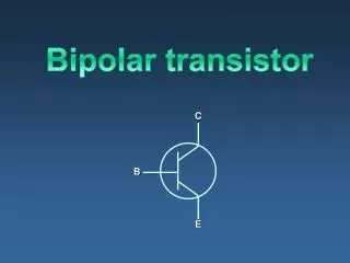
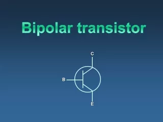
Bipolar transistor. § 3-1 Introduction. Bipolar Transistor. First bipolar transistor (BJT) was invented in 1948. The term bipolar came from the fact that both types of carriers, i.e., electron and hole play important roles in operation.

E N D
Bipolar transistor Physics of Semiconductor Devices
§3-1 Introduction Physics of Semiconductor Devices
Bipolar Transistor • First bipolar transistor (BJT) was invented in 1948 • The term bipolar came from the fact that both types of carriers, i.e., electron and hole play important roles in operation • Field Effect Transistor (FET) is unipolar, in which only one type of carrier is important Physics of Semiconductor Devices
Bipolar Transistor • In VLSI era, BJTs starts to lose their show stage due to the emergence of MOSFETs, which possess advantage of simplicity in term of process and circuit design • However, BJT’s refuse to step down because of their high current drive capability and superior analog performance (also useful in power applications) • Current trend is to combine the best of MOSFETs and Bipolar devices, which is known as BiCMOS process • BJT devices are also the preferred device for high speed (e.g. Emitter Couple Logic .ECL) and RF applications Physics of Semiconductor Devices
p n+ n n p+ p Bipolar Transistor Physics of Semiconductor Devices
Bipolar Transistor The ”Planar Process” developed by Fairchild in the late 50s shaped the basic structure of the BJT, even up to the present day. Physics of Semiconductor Devices
Modern BJT Physics of Semiconductor Devices
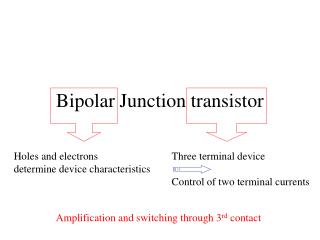
BJT basically consists of two neighbouring pn junctions back to back: • For apart enough that depletion regions don’t interact (no “punchthrough”) Uniqueness of BJT: high current drivability per input capacitance fast excellent for analog and front-end communications applications. • Close enough that minority carriers interact (negligible recombination in base) Physics of Semiconductor Devices
IC IB IE Bipolar operation Operation depends on the bias condition Physics of Semiconductor Devices
§3-2 Carrier distribution Physics of Semiconductor Devices
emitter current injected into the base base current injected into the emitter recombination in the base current region reverse biased current across the BCJ reverse biased current across the BCJ electron current from the emitter Current Flow Physics of Semiconductor Devices
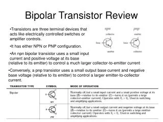
VEB VBE PNP NPN Forward active Forward active Saturation Saturation VCB VBC Inverted active Inverted active Cutoff Cutoff Mode C-B E-B active reverse forward inverted forward reverse saturation forward forward cutoff reverse reverse Bipolar Transistor Modes of operation Physics of Semiconductor Devices
An idealized p-n-p transistor in thermal equilibrium, that is ,where all there leads are connected together or all are ground. The impurity densities in the three doped regions, where the emitter is more heavily doped than the collector. However the base doping is less than the emitter doping, but greater than the collector doping. Physics of Semiconductor Devices
Transistor Action ACTIVE MODE In active mode, the emitter-base junction is forward biased and collector base-junction is reverse biased. Physics of Semiconductor Devices
Forward bias Reverse bias Electron Flow Hole Flow Current Flow Physics of Semiconductor Devices
Transistor Action Saturation Mode Both junction are in forward bias Cutoff Mode Both junctions are in reverse bias and all currents in the transistor are zero. Inverse-active Mode Junction between E and B is in forward bias and junction between B and C is in reverse bias. Physics of Semiconductor Devices
IE=IEp+IEn IC=ICp+ICn IB=IE-IC=IEn+(IEp-ICp)-ICn Current Gain Physics of Semiconductor Devices
Current Gain Common base current gain Emitter efficiency Base transport fact Physics of Semiconductor Devices
Collector current CB: current measured between these two terminals O: refers to the state of the third terminal with respect to the second Physics of Semiconductor Devices
Carrier Profile in Active Mode Physics of Semiconductor Devices
The device has uniform doping in each region. • The hole drift current in the base region as well as the collector saturation current is negligible. • There is low-level injection. • There are no generation-combination currents in the depletion region. • There are no series resistance in the devices. Carrier distribution in this region To derive the current-voltage expression for an ideal transistor, we assume the following: Physics of Semiconductor Devices
where and are the diffusion constant and the life time of minority carriers, respectively. Where is the diffusion length of holes. Carrier Distribution in each Region Base region Steady-state continuity equation The general solution is Physics of Semiconductor Devices
By the boundary conditions for the active mode: the solution can expressed When W/Lp<<1, the distribution equation can be simplified as Physics of Semiconductor Devices
Carrier distribution Physics of Semiconductor Devices
Carrier Distribution in each Region Emitter and collector region The boundary condition in the neutral region and collector region are: When nE0 and nC0 are the equilibrium electron concentrations in the emitter and collector, respectively. Substituting these boundary conditions into expressions similar to Eq.1 yields Physics of Semiconductor Devices
Active mode is BEJ forward biased while CBJ reverse biased • Saturation occurs when CBJ is forward biased • When IE=0, the device is cutoff, IC is the reverse leakage current ofthe CBJ. • Note that IC≠0 for VCB=0. The current is contributed by IE if the BEJ is forward biased. Common base Physics of Semiconductor Devices
Active mode for VBC=0. • Saturation mode with both junctions forward biased. Common base configuration Minority carrier distributions in the base region of a p-n-p transistor. Physics of Semiconductor Devices
Saturation occurs when both EBJ and CBJ are forward biased • Active mode is the most useful for linear applications • Saturation and cut-off modes are most useful for switching applications Common emitter Physics of Semiconductor Devices
Common emitter configuration Common emitter current gain Physics of Semiconductor Devices
§3-3 Current-voltage characteristics of ideal BJT Physics of Semiconductor Devices
Ideal BJT Physics of Semiconductor Devices
1D • Uniform doping distributions. • Minority carrier G&R in intrinsic base is negligible. • Emitter extrinsic base and collector also assumed “short” from minority carrier point of view. • Low level injection. • QNR thicknesses independent of VBE and VBC. • Ignore sidewall effects. • No parasitic resistances. • Ignore substrate. Ideal BJT simplifications: Physics of Semiconductor Devices
Simplified 1D model of intrinsic device: Physics of Semiconductor Devices
Regimes of operation: Physics of Semiconductor Devices
Basic operation in forward regime: Two junctions back-to-back: Physics of Semiconductor Devices
Injection of electrons from E to B Injection of holes from B to E VBE>0 Extraction of electrons from B to C Extraction of holes from C to B VBC<0 IB -IE>>IC Physics of Semiconductor Devices
Transistor effect: electrons injected from E to B, extracted by C Physics of Semiconductor Devices
In forward-active regime: • VBE controls IC (“transistor effect”) • IC independent of VBC (“isolation”) • Price to pay for control: IB Physics of Semiconductor Devices
Carrier profiles in TE and FAR: Physics of Semiconductor Devices
Dominant current paths in forward active regime: Physics of Semiconductor Devices
IC on VBE: , , none, other IC on VBC: , , none, other IB on VBE: , , none, other IB on VBC: , , none, other IC on IB: exponential, quadratic, none, other IC: electron injection from E to B and collection into C IB: hole injection from B to E IE=-IC-IB Key dependencies (choose one): Physics of Semiconductor Devices
Forward-active regime (VBE>0,VBC<0) Physics of Semiconductor Devices
Boundary conditions: Electron profile: Electron current density: Physics of Semiconductor Devices
Collector current scales with area of base-emitter junction AE: Physics of Semiconductor Devices
Collector saturation current Collector terminal current : or Physics of Semiconductor Devices
Base current: focus on hole injection and recombination in emitter (assume “short” or “transparent” and S= at surface) Physics of Semiconductor Devices
Boundary conditions: Hole profile: Hole current density: Physics of Semiconductor Devices
Base current scales with area of base-emitter junction AE: Base terminal current: Physics of Semiconductor Devices