1 / 6
60 likes | 70 Views
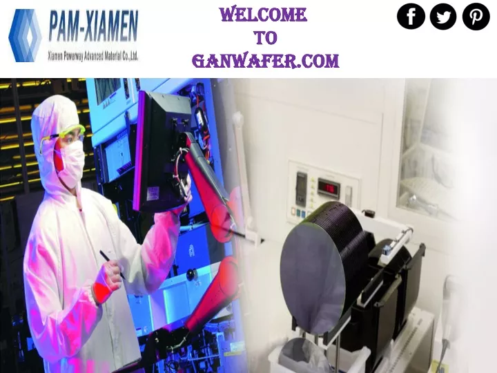
We specialize in the research and production of compound semiconductor wafers such as SiC&GaN material (SiC wafer and epitaxy, GaN wafer and epi wafer) and III-V material (III-V substrate and epi service: InP wafer, GaSb wafer, GaAs wafer, InAs wafer, and InSb wafer).

E N D
WELCOME TO GANWAFER.COM
GaN on Silicon HEMT Wafer PAM-XIAMEN offers GaN on Silicon HEMT structure and template, including GaN HEMT Wafer on Silicon, D-mode; GaN HEMT Wafer on Silicon, E-mode; GaN HEMT Wafer on Silicon for RF Application; GaN on Silicon Template. GaN based power electronic devices are still very expensive compared with Si devices. One of the ways to solve the cost problem is to fabricate GaN based heterostructures by epitaxy on Si substrate, and then to fabricate GaN based devices by complementary metal oxide semiconductor (CMOS) technology, so that the cost performance of the devices is better than that of Si devices.
SiC Wafers PAM-XIAMEN offers semiconductor SiC wafer Substrate, 6H SiC and 4H SiC (Silicon Carbide) in different quality grades for researcher and industry manufacturers. We has developed SiC crystal growth technology and SiC crystal wafer processing technology,established a production line to manufacturer SiC substrate, Which is applied in GaNepitaxy device, power devices, high-temperature device and optoelectronic Devices.
III-V Epi wafer We offer III-V Epi service based on GaAs Substrate, InPsubstrate, GaSb Substrate, InAs Substrate, and InSb substrate, in different types of epi wafer by MBE or MOCVD. We supply custom structures to meet customer specifications. Please contact us for more information.
Germanium Wafer In the germanium wafer production process, germanium dioxide from the residue processing is further purified in chlorination and hydrolysis steps. 1. High purity germanium is obtained during zone refining. 2. A germanium crystal is produced via the Czochralski process. 3. The germanium wafer is manufactured via several cutting, grinding, and etching steps. 4. The wafers are cleaned and inspection. During this process, the wafers are single side polished or double side polished according to custom requirement, epi-ready wafer comes. 5. The wafers are packed in single wafer containers, under a nitrogen atmosphere.
Xiamen Powerway Advanced Material Co., Ltd Address: Henghui Business Center,No.77,Lingxia Nan Road, High Technology Zone, Huli, Xiamen, Fujian, 361006 China Call: +86-592-5601 404 Fax: +86-592-5563 272 Email: tech@powerwaywafer.com Website: http://www.ganwafer.com/