Download

1 / 19
290 likes | 857 Views
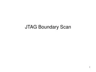
T. T. internal. internal. A. A. logic. logic. P. P. TDI. TDI. T. TDO. internal. T. TMS. TMS. A. logic. A. TCK. TCK. P. P. TDO. TDO. Data_in. T. internal. internal. logic. logic. A. P. TDI. TDO. BSC. Data_out. Boundary Scan Architecture. Data Registers.

E N D
T T internal internal A A logic logic P P TDI TDI T TDO internal T TMS TMS A logic A TCK TCK P P TDO TDO Data_in T internal internal logic logic A P TDI TDO BSC Data_out Boundary Scan Architecture
Data Registers Scan Boundary Registers Internal logic TDI Device ID. Register Bypass Register TDO Instruction Register (IR) Boundary Scan Architecture
To next cell To system logic From system pin 0 1 0 SET SET SET SET D D D D Q Q Q Q 1 Test/Normal Q Q Q Q CLR CLR CLR CLR From last cell Clock DR Update DR Shift DR Boundary Scan Cell Used at the input or output pins
Boundary Scan Working Modes SAMPLE mode: Get snapshot of normal chip output signals
Boundary Scan Working Modes PRELOAD mode: Put data on boundary scan chain before next instruction
Boundary Scan Working Modes Extest instruction: Test off-chip circuits and board-level interconnections
Boundary Scan Working Modes INTEST instruction Feeds external test patterns in and shifts responses out
From TDI SET Q D Shift DR To TDO Q Clock DR CLR Boundary Scan Working Modes Bypass instruction: Bypasses the corresponding chip using 1-bit register
Boundary Scan Working Modes IDCODE instruction: Connects the component device identification register serially between TDI and TDO in the Shift-DR TAP controller state Allows board-level test controller or external tester to read out component ID Required whenever a JEDEC identification register is included in the design TDO TDI Version Part Number Manufacturer ID 1 4-bits Any format 11-bits Coded form of JEDEC 16-bits Any format
Short Open Fault Diagnosis with Boundary Scan 1 0 0 0 Assume wired AND 1 0 Assume stuck-at-0
Short 10 00 01 00 Assume wired AND 00 00 11 Open 00 Assume stuck-at-0 Fault Diagnosis with Boundary Scan Kautz showed in 1974 that a sufficient condition to detect any pair of short circuited nets was that the “horizontal” codes must be unique for all nets. Therefore the test length is]log2(N)[
Short Open Fault Diagnosis with Boundary Scan 101 001 011 001 Assume wired AND 001 001 000 110 Assume stuck-at-0 All 0-s and all 1-s are forbidden codes because of stuck-at faults Therefore the final test length is]log2(N+2)[
Short Open Fault Diagnosis with Boundary Scan 0 101 0 001 0 001 0 011 Assume wired AND 1 001 1 001 0 000 1 110 Assume stuck-at-0 To improve the diagnostic resolution we have to add one bit more
Synthesis of Testable Circuits Test generation: x1 x2 x3 y x1 & & x3 y 1 & 0 1 1 0 1 0 0 0 1 0 0 1 0 1 1 0 1 1 0 0 0 0 1 1 0 0 1 1 1 1 1 1 x2 & 4 test patterns are needed
Synthesis of Testable Circuits Two implementations for the same circuit: x1 x2 x3 010 110 010 & x1 110 y & & x3 101 y 1 & & 110 x2 & First assignment Here: Only 3 test patterns are needed Here: 4 test patterns are needed
Synthesis of Testable Circuits Given: Calculation of constants: New: fi x1 x2 x3 y f0 0 0 0 1 1 C0 = f0 f1 0 0 1 0 1 C1 = f0 f1 f2 0 1 0 1 0 C2 = f0 f2 f3 0 1 1 0 0 C3 = f0 f1 f2 f3 f4 1 0 0 0 1 C4 = f0 f4 f5 1 0 1 0 1 C5 = f0 f1 f4 f5 f6 1 1 0 1 1 C6 = f0 f2 f4 f6 f7 1 1 1 1 0 C3 = f0 f1 f2 f3 f4 f5 f6 f7
Synthesis of Testable Circuits Test generation method: Roles of test patterns: 1 & x1 x2 x3 x1 x2 x3 011 110 0 0 0 1 1 1 0 1 1 1 0 1 1 1 0 0 & 0 011 & 110 y 101 & 110 1 &
Testability as a trade-off Theorem: You can test an arbitrary digital system by only 3 test patterns if you design it approprietly Amusing testability: Proof: 011 011 001 & & 001 & 101 101 ? 011 001 & 011 1 101 & 010 001 101 Solution: System FSM Scan-Path CC NAND