Digital Fundamentals with PLD Programming Floyd
520 likes | 1.4k Views
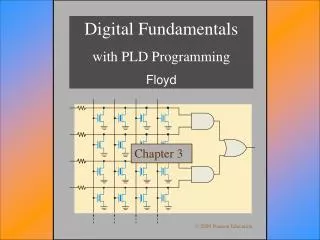
Digital Fundamentals with PLD Programming Floyd. Chapter 3. © 2009 Pearson Education. The NOT operation (complement) is shown with an overbar. Thus, the Boolean expression for an inverter is X = A . Summary. A. X. The Inverter.

Digital Fundamentals with PLD Programming Floyd
E N D
Presentation Transcript
Digital Fundamentals with PLD Programming Floyd Chapter 3 © 2009 Pearson Education
The NOT operation (complement) is shown with an overbar. Thus, the Boolean expression for an inverter is X =A. Summary A X The Inverter The inverter performs the Boolean NOT operation. When the input is LOW, the output is HIGH; when the input is HIGH, the output is LOW. LOW (0) HIGH (1) HIGH (1) LOW(0)
Summary A X The Inverter Example waveforms: A X A group of inverters can be used to form the 1’s complement of a binary number: Binary number 1 0 0 0 1 1 0 1 0 1 1 1 0 0 1 0 1’s complement
Summary A A X X The AND Gate B B The AND gate produces a HIGH output when all inputs are HIGH; otherwise, the output is LOW. For a 2-input gate, the truth table is 0 0 0 1 1 0 1 1 0 0 0 1 The AND operation is usually shown with a dot between the variables but it may be implied (no dot). Thus, the AND operation is written as X = A .B or X = AB.
Summary A A X X The AND Gate B B Example waveforms: A B X The AND operation is used in computer programming as a selective mask. If you want to retain certain bits of a binary number but reset the other bits to 0, you could set a mask with 1’s in the position of the retained bits. If the binary number 10100011 is ANDed with the mask 00001111, what is the result? Example 00000011
Summary The AND Gate Example A Multisim circuit is shown. XWG1 is a word generator set in the count down mode. XLA1 is a logic analyzer with the output of the AND gate connected to first (upper) line of the analyzer. What signal do you expect to on this line? Solution The output (line 1) will be HIGH only when all of the inputs are HIGH.
Summary A X A X The OR Gate B B The OR gate produces a HIGH output if any input is HIGH; if all inputs are LOW, the output is LOW. For a 2-input gate, the truth table is 0 0 0 1 1 0 1 1 0 1 1 1 The OR operation is shown with a plus sign (+) between the variables. Thus, the OR operation is written as X = A + B.
Summary A X A X The OR Gate B B Example waveforms: A B X The OR operation can be used in computer programming to set certain bits of a binary number to 1. ASCII letters have a 1 in the bit 5 position for lower case letters and a 0 in this position for capitals. (Bit positions are numbered from right to left starting with 0.) What will be the result if you OR an ASCII letter with the 8-bit mask 00100000? Example Solution The resulting letter will be lower case.
Summary The OR Gate A Multisim circuit is shown. XWG1 is a word generator set to count down. XLA1 is a logic analyzer with the output Example connected to first (top) line of the analyzer. The three 2-input OR gates act as a single 4-input gate. What signal do you expect on the output line? The output (line 1) will be HIGH if any input is HIGH; otherwise it will be LOW. Solution
The NAND operation is shown with a dot between the variables and an overbar covering them. Thus, the NAND operation is written as X = A .B (Alternatively, X = AB.) Summary A A X X The NAND Gate B B The NAND gate produces a LOW output when all inputs are HIGH; otherwise, the output is HIGH. For a 2-input gate, the truth table is 0 0 0 1 1 0 1 1 1 1 1 0
Summary A A X X The NAND Gate B B Example waveforms: A B X The NAND gate is particularly useful because it is a “universal” gate – all other basic gates can be constructed from NAND gates. How would you connect a 2-input NAND gate to form a basic inverter? Question
Summary The NAND Gate Example A Multisim circuit is shown. XWG1 is a word generator set in the count up mode. A four-channel oscilloscope monitors the inputs and output. What output signal do you expect to see? Solution The output (channel D) will be LOW only when all of the inputs are HIGH. Inputs
The NOR operation is shown with a plus sign (+) between the variables and an overbar covering them. Thus, the NOR operation is written as X = A + B. Summary A X A X The NOR Gate B B The NOR gate produces a LOW output if any input is HIGH; if all inputs are HIGH, the output is LOW. For a 2-input gate, the truth table is 0 0 0 1 1 0 1 1 1 0 0 0
Summary A X A X The NOR Gate B B Example waveforms: A B X The NOR operation will produce a LOW if any input is HIGH. Example When is the LED is ON for the circuit shown? Solution The LED will be on when any of the four inputs are HIGH.
The XOR operation is written as X = AB + AB. Alternatively, it can be written with a circled plus sign between the variables as X = A + B. Summary A X A X The XOR Gate B B The XOR gate produces a HIGH output only when both inputs are at opposite logic levels. The truth table is 0 0 0 1 1 0 1 1 0 1 1 0
Summary A X A X The XOR Gate B B Example waveforms: A B X Notice that the XOR gate will produce a HIGH only when exactly one input is HIGH. If the A and B waveforms are both inverted for the above waveforms, how is the output affected? Question There is no change in the output.
The XNOR operation shown as X = AB + AB. Alternatively, the XNOR operation can be shown with a circled dot between the variables. Thus, it can be shown as X = A . B. Summary A X A X The XNOR Gate B B The XNOR gate produces a HIGH output only when both inputs are at the same logic level. The truth table is 0 0 0 1 1 0 1 1 1 0 0 1
Summary A X A X The XNOR Gate B B Example waveforms: A B X Notice that the XNOR gate will produce a HIGH when both inputs are the same. This makes it useful for comparison functions. If the A waveform is inverted but B remains the same, how is the output affected? Question The output will be inverted.
Summary Fixed Function Logic Two major fixed function logic families are TTL and CMOS. A third technology is BiCMOS, which combines the first two. Packaging for fixed function logic is shown. DIP package SOIC package
Summary Fixed Function Logic Some common gate configurations are shown.
Summary Fixed Function Logic Logic symbols show the gates and associated pin numbers.
Summary Fixed Function Logic Data sheets include limits and conditions set by the manufacturer as well as DC and AC characteristics. For example, some maximum ratings for a 74HC00A are:
Summary Programmable Logic A Programmable Logic Device (PLD) can be programmed to implement logic. There are various technologies available for PLDs. Many use an internal array of AND gates to form logic terms. Many PLDs can be programmed multiple times.
Summary Programmable Logic In general, the required logic for a PLD is developed with the aid of a computer. The logic can be entered using a Hardware Description Language (HDL) such as VHDL. Logic can be specified to the HDL as a text file, a schematic diagram, or a state diagram. A text entry for a programming a PLD in VHDL as a 2-input NAND gate is shown for reference in the following slide. In this case, the inputs and outputs are first specified. Then the signals are described. Although you are probably not familiar with VHDL, you can see that the program is simple to read. Example
Summary Programmable Logic entity NandGate is port(A, B: in bit; LED: out bit); end entity NandGate; architecture GateBehavior of NandGate is signal A, B: bit; begin X <= A nand B; LED <= X; end architecture GateBehavior;
Selected Key Terms A logic circuit that inverts or complements its inputs. Inverter Truth table Timing diagram Boolean algebra AND gate A table showing the inputs and corresponding output(s) of a logic circuit. A diagram of waveforms showing the proper time relationship of all of the waveforms. The mathematics of logic circuits. A logic gate that produces a HIGH output only when all of its inputs are HIGH.
Selected Key Terms A logic gate that produces a HIGH output when one or more inputs are HIGH. OR gate NAND gate NOR gate Exclusive-OR gate Exclusive-NOR gate A logic gate that produces a LOW output only when all of its inputs are HIGH. A logic gate that produces a LOW output when one or more inputs are HIGH. A logic gate that produces a HIGH output only when its two inputs are at opposite levels. A logic gate that produces a LOW output only when its two inputs are at opposite levels.
Quiz • The truth table for a 2-input AND gate is 0 0 0 1 1 0 1 1 0 1 1 0 0 0 0 1 1 0 1 1 1 0 0 0 a. b. 0 0 0 1 1 0 1 1 0 0 0 1 0 0 0 1 1 0 1 1 0 1 1 1 c. d. © 2009 Pearson Education
Quiz • The truth table for a 2-input NOR gate is 0 0 0 1 1 0 1 1 0 1 1 0 0 0 0 1 1 0 1 1 1 0 0 0 a. b. 0 0 0 1 1 0 1 1 0 0 0 1 0 0 0 1 1 0 1 1 0 1 1 1 c. d. © 2009 Pearson Education
Quiz • The truth table for a 2-input XOR gate is 0 0 0 1 1 0 1 1 0 1 1 0 0 0 0 1 1 0 1 1 1 0 0 0 a. b. 0 0 0 1 1 0 1 1 0 0 0 1 0 0 0 1 1 0 1 1 0 1 1 1 c. d. © 2009 Pearson Education
Quiz A X 4. The symbol is for a(n) B a.OR gate b. AND gate c. NOR gate d. XOR gate © 2009 Pearson Education
Quiz A X 5. The symbol is for a(n) B a.OR gate b. AND gate c. NOR gate d. XOR gate © 2009 Pearson Education
Quiz 6. A logic gate that produces a HIGH output only when all of its inputs are HIGH is a(n) a.OR gate b. AND gate c. NOR gate d. NAND gate © 2009 Pearson Education
Quiz 7. The expression X = A + B means a. A OR B b. A AND B c. A XOR B d. A XNOR B © 2009 Pearson Education
Quiz 8. A 2-input gate produces the output shown. (X represents the output.) This is a(n) a.OR gate b. AND gate c. NOR gate d. NAND gate A B X © 2009 Pearson Education
Quiz 9. A 2-input gate produces a HIGH output only when the inputs agree. This type of gate is a(n) a.OR gate b. AND gate c. NOR gate d. XNOR gate © 2009 Pearson Education
Quiz 10. The required logic for a PLD can be specified in an Hardware Description Language by a. text entry b. schematic entry c. state diagrams d. all of the above © 2009 Pearson Education
Quiz Answers: 1. c 2. b 3. a 4. a 5. d 6. b 7. c 8. d 9. d 10. d