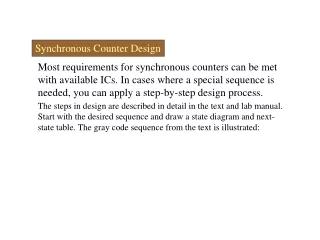
Synchronous Counter
Synchronous Counter. Synchronous Counter. This presentation will Define synchronous counters . Provide examples of 3-Bit and 4-Bit synchronous up counters. Provide examples of 3-Bit and 4-Bit synchronous down counters. Synchronous Counters.


Synchronous Counter
E N D
Presentation Transcript
Synchronous Counter This presentation will • Define synchronous counters. • Provide examples of 3-Bit and 4-Bit synchronous up counters. • Provide examples of 3-Bit and 4-Bit synchronous down counters.
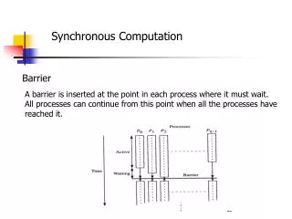
Synchronous Counters • All flip-flops are simultaneously clocked by an external clock. • Synchronous counters are faster than asynchronous counters of the simultaneous clocking. • Synchronous counters do not suffer from the ripple effect that asynchronous counters do. • Synchronous counters require more logic an asynchronous counters.
3-Bit Synch Up Counter: Theory Q0 : Toggles On Falling Edge of CLOCK Q1 : Toggles On Falling Edge of CLOCK & Q0=1 Q2 : Toggles On Falling Edge of CLOCK & Q0=1 & Q1=1
3-Bit Synch Up Counter: Circuit Toggles On: Falling Edge of CLOCK Toggles On: Falling Edge of CLOCK AND Q0=1 Toggles On: Falling Edge of CLOCK AND Q0=1 & Q1=1
3-Bit Synch Up Counter: Timing “0” “1” “2” “3” “4” “5” “6” “7” Q2 Q1 Q0 CLK
4-Bit Synch Up Counter: Circuit Toggles On: Falling Edge of CLOCK Toggles On: Falling Edge of CLOCK AND Q0=1 Toggles On: Falling Edge of CLOCK AND Q0=1 & Q1=1 Toggles On: Falling Edge of CLOCK AND Q0=1 & Q1=1 & Q2=1
3-Bit Synch Down Counter: Theory Q0 : Toggles On Falling Edge of CLOCK Q1 : Toggles On Falling Edge of CLOCK & Q0=0 Q2 : Toggles On Falling Edge of CLOCK & Q0=0 & Q1=0
3-Bit Synch Down Counter: Circuit Toggles On: Falling Edge of CLOCK Toggles On: Falling Edge of CLOCK AND Q0=0 Toggles On: Falling Edge of CLOCK AND Q0=0 & Q1=0
4-Bit Synch Down Counter: Circuit Toggles On: Falling Edge of CLOCK Toggles On: Falling Edge of CLOCK AND Q0=0 Toggles On: Falling Edge of CLOCK AND Q0=0 & Q1=0 Toggles On: Falling Edge of CLOCK AND Q0=0 & Q1=0 & Q2=0
Synchronous MSI Counter This presentation will • Introduce the 74LS163 Synchronous 4-Bit Binary Up Counter. • Review the 74LS163’s connection diagrams, signal descriptions, logic and timing diagrams. • Provide an examples of a counter application implemented with the 74LS163. • Introduce the 74LS193 Synchronous 4-Bit Binary Up/Down Counter. • Review the 74LS193’s connection diagrams, signal descriptions, logic and timing diagrams. • Provide an examples of a counter application implemented with the 74LS193.
74LS163 Synchronous Binary Up Counter • Four Bit Synchronous Up Counting. • Pre-loadable Count Start • Synchronous Load • Synchronous Clear • Two Count Enable Inputs • Carry-Out Signal for Counter Cascading
74LS163 Component Diagram 74LS163 Component Diagram From CDS 74LS163 Connection Diagram From Datasheet
74LS163 Signal Descriptions(1 of 2) Signal Name: • A : Data Input (LSB) • B : Data Input • C : Data Input • D : Data Input (MSB) • QA : Data Output (LSB) • QB : Data Output • QC : Data Output • QD : Data Output (MSB)
74LS163 Signal Descriptions(2 of 2) Signal Name: • ENP : Count Enable P • ENT : Count Enable T • LOAD : Data Load • CLEAR : Clears The Counter • CLOCK : Clock Input • RCO : Ripple Carry Out
74LS163 Timing Diagram(1 of 3) • CLEAR set to a logic (0); Outputs are cleared on next rising edge of clock. • LOAD set to a logic (0); Outputs are loaded with input data on next rising edge of clock. In this example a 12 (1100) is loaded. B A
74LS163 Timing Diagram(2 of 3) • Counting is enabled; ENT & ENP are both set to a logic (1). On every rising edge of clock, the output count is incremented by one. In this example 12, 13, 14, 15, 0, 1, 2. Note, when the count is 15, RCO is a logic (1) for the full clock cycle . C
74LS163 Timing Diagram(3 of 3) • ENP set to a logic (0); Counting is disabled. • ENT set to a logic (0); Counting is disabled. D E
74LS163 Design Example #1 “0” “1” “2” “3” “4” “5” “6” “E” “F” “0” “7” “8” “9” “A” “B” “C” “D” RCO QD QC QB QA CLK Repeats →
74LS163 Design Example #2 “B” “C” “D” “3” “4” “5” “6” “3” “4” “5” “7” “8” “9” “A” “B” “C” “D” RCO QD QC QB QA LOAD CLK Repeats →
74LS193 Synchronous Binary Up/Down Ctr • Four Bit Synchronous Up / Down Counting. • Separate Clock Inputs for Up & Down Counting • Pre-loadable Count Start • Asynchronous Load • Asynchronous Clear • Carry-Out Signal for Counter Cascading Up Counters • Borrow-Out Signal for Counter Cascading Down Counters
74LS193 Component Diagram 74LS193 Component Diagram From CDS 74LS193 Connection Diagram From Datasheet
74LS193 Signal Descriptions(1 of 2) Signal Name: • A : Data Input (LSB) • B : Data Input • C : Data Input • D : Data Input (MSB) • QA : Data Output (LSB) • QB : Data Output • QC : Data Output • QD : Data Output (MSB)
74LS193 Signal Descriptions(2 of 2) Signal Name: • UP : Up Counter Clock Input • DOWN : Down Counter Clock Input • ~LOAD : Data Load • CLR : Clears The Counter • ~BO : Borrow Output • ~CO : Carry Output
74LS193 Timing Diagram(1 of 3) • CLEAR set to a logic (1); Outputs are cleared immediately. CLEAR is an asynchronous input. • LOAD set to a logic (0); Outputs are loaded with input data immediately. In this case13 (1101). LOAD is an asynchronous input. B A
74LS193 Timing Diagram(2 of 3) • COUNT UP is clocked and COUNT DOWN is a logic (1). On every rising edge of clock, the output count is incremented by one. In this example 13, 14, 15, 0, 1, 2. Note, when the count is 15, CARRY is a logic (0) for ½ the clock cycle . C
74LS193 Timing Diagram(3 of 3) • COUNT DOWN is clocked and COUNT UP is a logic (1). On every rising edge of clock, the output count is decremented by one. In this example 2, 1, 0, 15, 14, 13. Note, when the count is 0, BORROW is a logic (0) for ½ the clock cycle . D
74LS193 Design Example #1 “C” “D” “E” “F” “0” “1” “2” “3” “4” “5” “6” “7” “8” “9” “A” “B” “C” “D” “E” “F” “0” “1” “2” “3” CO BO QD QC QB QA CLK Repeats →
74LS193 Design Example #2 “3” “2” “1” “0” “F” “E” “D” “C” “B” “A” “9” “8” “7” “6” “5” “4” “3” “2” “1” “0” “F “E” “D” “C” CO BO QD QC QB QA CLK Repeats →
74LS193 Design Example #2 “5” “4” “3” “D” “C” “B” “A” “D” “C” “9” “8” “7” “6” “5” “4” “3” RCO QD QC QB QA LOAD CLK Repeats →