Download
1 / 34
340 likes | 371 Views
Explore the 68HC11 Timer System features for I/O operations - from Real Time Clock to Output Compare functions. Learn how the system functions and how to make the most of its capabilities.

E N D
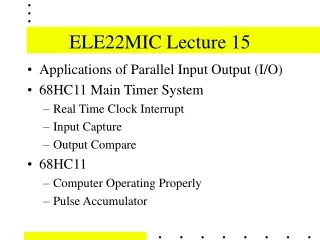
ELE22MIC Lecture 15 • Applications of Parallel Input Output (I/O) • 68HC11 Main Timer System • Real Time Clock Interrupt • Input Capture • Output Compare • 68HC11 • Computer Operating Properly • Pulse Accumulator
68HC11 Timer System (1) • The HC11 Timer System is based on a free-running 16 bit counter with a four stage programmable pre-scaler. • Three Independent Input Capture functions can be used to record the count when a transition is detected on inputs IC1, IC2, or IC3 • Five Output Compare functions are included for generating software timing delays or output signals on pins OC1, OC2, OC3, OC4 and OC5
68HC11 Timer System (2) • A programmable periodic interrupt circuit called Real Time Interrupt (RTI) • A Computer Operating Properly (COP) watchdog function is also related to this timer circuit. • There are over 6 x 1-byte registers, and 9 x double-byte registers associated with the Timer system
68HC11 Timer System (3) • Timer Register Summary: • TCNT - 2-byte Free Running Timer Counter Value • TOCx/TICx - 8 x 2-byte TIC/TOC count registers • 5 for Timer Ouput Compare & 4 Timer Input Capture (One shared TIC/TOC) • TMSK1 - 1 byte - Timer Interrupt Enables • TMSK2 - $1024 - PR0/PR1/RTI • OPTION - $1039 - CR0/CR1 - Clock Pre-scaler • CFORC - 1 x byte port for Force output compare • TCTL2 - 1 x byte register for output port control OMx/OLx • TFLG1 - 1 x byte flag register indicating state of comparisons
68HC11 Timer - PreScaler • An E-Clock PreScaler divides by 1, 4, 8 or 16 • This value is selected by writing to Bits PR0, PR1 of the TMSK2 register (at $1024). • In normal modes the pre-scale rate may only be changed once within the first 64 bus cycles after reset.
68HC11 Timer - PreScaler • Crystal Frequency vs clock Pre-Scaler
Free Running Counter - TCNT (1) • The pre-scaled clock clocks a free-running counter, TCNT (= $100E..$100F) • The TCNT Count Value can be read using the instructions: • LDD $100E Reads all 16 Bits in one instruction. • The Timer value is frozen during this instruction sequence. • DONT read the timer with the following instruction sequence: • LDAA $100E • LDAB $100F • as the counter will be incremented between the instructions
Free Running Counter - TOF (3) • Timer Overflow Flag - TOF • Bit 7 of TFLG2 register = $1025 • TOF is Set when the timer counts from $FFFF -> $0. • This can be used for extending the range of the count by incrementing a separate counter. • TOF bit must be reset by writing a one to the TOF bit (bit-7 of the TFLG2 register).
Free Running Counter - TOI (3) • A Timer Overflow Interrupt • TOI = Bit 7 in TMSK2 register = $1024 • TOI may be enabled to facilitate greater counter range under interrupt control. • Refer Section 10.2 of HC11 Ref. Manual
Timer Output Compare - TOC (1) • The five Output Compare pins can be used independently to create precise timing for time delays or external logic pulses. • Each Output Compare Register is compared to the value in the 16 bit counter, and if equal, triggers its Timer Output Compare (TOCn) function.
Timer Output Compare (2) • The output compare hardware can ensure that intervals and waveforms are not subject to jitter due to interrupt servicing routines
Timer Output Compare (3) • TCTL2 $1020, OM2 & OL2 - select the relationship of Output Compare to Output Port Pin OMx OLx where x = 2..5 0 0 No Change 0 1 Toggle Pin state 1 0 Force Pin to 0 1 1 Force Pin to 1
TOC code (4) REGBAS EQU $1000 * Starting address for register block PORTB EQU $04 * Output port B TCNT EQU $0E * Free running counter (16 bit) TOC2 EQU $18 * OC2 register (16 bit) TCTL1 EQU $20 * OM2,OL2,OM3,OL3;OM4,OL4,OM5,OL5 TCTL2 EQU $21 * -,-,EDGlB,EDGlA,EDG2B,EDG2A,EDG3B, * EDG3A TMSK1 EQU $22 * OC1I,OC2I,OC3I,OC4I;OC51,IC1I,IC2I,IC3I TFLG1 EQU $23 *OC1F,OC2F,OC3F,OC4F;OC5F,IC1F,IC2F,IC3F TMSK2 EQU $24 * TOI,RTII,PAOVI,PAII;-,-,PR1,PR0 TFLG2 EQU $25 * TOF,RTIF,PAOVF,PAIF;-,-,-,- *** EVB Routine Addresses & Pseudo Vector Equates PVOC2 EQU $00DC EVB Pseudo Vector for OC2 ORG $2000 Start variables in RAM (upper half) HDLY RMB 2 Half-cycle delay (in 0.5mS increments)
TOC code (5) TOP5 LDS #$0047 * Top of User’s Stack area on EVB LDAA #$7E * Jump (extended) Opcode STAA PVOC2 * Pseudo Vector see manual text LDX #SV5OC2 * Address of OC2 service routine STX PVOC2+1 * Finish jump instruc to TOF svc LDX #REGBAS * Point to register block LDAA #%01000000 * OM2:OL2 = 0:1 STAA TCTL1,X * Set OC2 for toggle, on compare STAA TFLG1,X * Clear any pending,OC2F STAA TMSK1,X * Enable OC2 interrupts CLI * Enable Interrupts BRA * * Interrupt driven; sit here * Try varying hdly
TOC code (6) *** * SV5OC2 - Output Compare 2 Interrupt Service Routine (ISR) * * Called at each OC2 interrupt. *** SV5OC2 LDD HDLY * Get delay time for 1/2 cycle ADDD TOC2,X * Add HDLY to last compare value STD TOC2,X * Update OC2 (schedule next edge) BCLR TFLG1,X $BF * Clear OC2F RTI ** Return from OC2 service **
Timer Input Capture - TIC • The three Input Capture pins can be used independently to measure period or pulse-width of the signal. • Refer Section 10.1.2 of Motorola HC11 Reference Manual for detail.
68HC11 Timer System • Input Capture Control - Edge Polarity
68HC11 Timer System • The Input-Capture pin x can be configured to be sensitive to • Capture disabled EDGxB = 0, EDGxA=0 • Rising Edges EDGxB = 0, EDGxA=1 • Falling Edges EDGxB = 1, EDGxA=0 • Any Edge EDGxB = 1, EDGxA=1
Measuring Period (1) • The period of a signal can be measured by counting cycles between two successive rising edges of an Input Capture pin. • The time count on the free running timer TCNT can be configured to be latched on a rising edge of PortA2 = Pin IC1. • The cpu can then poll the status register until IC1 has latched a value, then read and save this count value
Measuring Period (2) • Next the cpu can wait until the next rising edge of IC1 latches the next value. • The cpu can again poll the status register until IC1 has latched a value, then read and save this count value • The difference in counts is the number of clock cycles elapsed. • There is a minimum measurable period of 26 cycles due to the following software
Measuring Period - Code(3) * Ready to detect first rising edge BRCLR TFLG1,X $04 * Loop here until first edge detected LDD TIC1,X * Read time of first edge STD FIRSTE * Save first captured edge value LDAA #$04 STAA TFLG1,X * Clear IC1F before next edge * Ready to capture time of second edge BRCLR TFLG1,X $04 * Loop here until second edge detected LDD TIC1,X * Read time of second edge SUBD FIRSTE * 2nd - 1st -> D check for BCC NoWrap NEGD NoWrap: STD PeriodCyc * Save result (period in cycles) * Adapted from Motorola M68HC11 Reference Manual P10-18
Computer Operating Properly (1) • The COP Watchdog is intended to detect software processing errors. • When COP is enabled, the software is responsible for preventing a free-running watchdog timer from timing out. • If the COP timer times out, this indicates that the software is no longer operating correctly, and so a system reset is initiated.
Computer Operating Properly (2) • The OPTION register contains the CR1/CR0 bits used to set the COP Timer Rate Select Bits.
Computer Operating Properly (3) • If the COP Watchdog is enabled, then the watchdog must be acknowledged within the time-out period to avoid being reset. • The COP Watchdog is enabled if the NOCOP control bit in the CONFIG register is cleared. • The CONFIG register is held in an EEPROM cell.
Computer Operating Properly (4) • To acknowledge that the software is operating properly software must: • 1. Write $55 to the COPRST register to arm the COP timer-clearing mechanism • 2. Write $AA to the COPRST register which then clears the COP timer. • This inhibits reset, and clears the COP timer to start another cycle. • This process is called “servicing the COP timer”.
Computer Operating Properly (5) • The COP service code should be placed in the main program in a place which can only be reached after normal program functioning is confirmed. • As the COP timer is based on the MCU clock, the watchdog cannot detect errors that cause the MCU clock to SLOW or STOP altogether. • A separate Clock Monitor Reset can be used to force reset if the MCU clock stops.
Computer Operating Properly (6) • In the event that the MPU Latches-up, neither COP timeout nor Clock Monitor reset will reset the CPU. • With CMOS latch-up, a parasitic thryristor is created. As with all thryristors, the main method to stop latch-up is to remove current - i.e. cycle the power off then on again. • If your device must restart reliably after failure, a power cycling circuit may be required.
Reset Vectors vs Cause Bootstrap mode: In this mode a small on-chip ROM is enabled at address $BF40..BFFF. The reset vector is fetched from bootstrap ROM. The firmware checks the security option (no security if SMOD bit = 0), and accepts a 256 byte program through the Serial Communications Interface (SCI) then jumps to the program loaded at $0000 on the on-chip RAM. Refer Section 3.5.4 HC11 Reference Manual
Variable Speed Stepper Motor • The next application we will look at is a Variable Speed Stepper Motor control • The forward/reverse speed is controlled by a potentiometer connected to the ADC input • The unsigned potentiometer value 0..255 is biased by 128 so that mid-way = 0 speed, 127 = full speed forwards, -127 = full speed reverse. • The stepper motor coil activation sequence is controlled by four output lines of Port A
Pulse Accumulator • The Pulse accumulator is an 8-bit counter configured to act as a simple event counter or for gated time accumulation. • The Pulse accumulator can operate in one of two basic modes: • Event Counting • Gated time accumulation • Refer Section 11 of Motorola HC11 Reference Manual for detail.
Pulse Accumulator • Event Counting mode • On each active edge of the PAI pin, the 8-bit counter is incremented.
Pulse Accumulator • Gated Time Accumulation mode • The 8-bit counter is clocked by a free-running E divided by 64 clock while PAI is active
Acknowledgments • Images of the configuration registers, and some source code examples, are derived from the Motorola M68HC11 Reference Manual