Download

1 / 24
240 likes | 407 Views
Understanding the Physics of Plasma Display Addressing. Vladimir Nagorny (available at www.plasmadynamics.com). Addressing Speed and Cost. Cost is the name of the game today Single-scan Frame - 16.7 ms ≥ 10 Subfields, ~1000 lines) Reset ~ 1.5-3 ms Sustain > 5-6ms, or it is dim

E N D
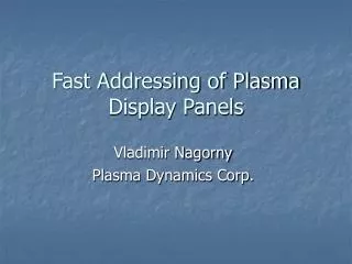
Understanding the Physics of Plasma Display Addressing Vladimir Nagorny (available at www.plasmadynamics.com)
Addressing Speed and Cost • Cost is the name of the game today • Single-scan Frame - 16.7ms≥10 Subfields, ~1000 lines) • Reset ~ 1.5-3ms • Sustain > 5-6ms, or it is dim • Address ~ 7.7-10.2ms 0.75-1ms/line for single scan HDTV addressing
Three periods - three components • Each period has its purpose, its specifics (priming, wall charges), requirements (stability, efficiency, speed) and problems. • The purpose of the setup period is to place all cells into identical and known state. Usually it is in the corner of the Vt-curve, where either PG or both PG and SG discharges are active • The purpose of address period is to do the opposite -to discriminate between ON and OFF cells, so that one can start sustaining of the ON and not the OFF cells • The purpose of sustaining period are to produce picture (light) and provide priming
Starting point for addressing • Assume that at the end of the reset period both SG and PG or at least PG discharges are active and ramp is stable. Cell is in the corner of Vt-curve – breakdown boundary for 3 electrodes, which can be verified by measuring the Vt-curve. After that every cell is “locked”. • For addressing one unlocks line by line and addresses it. Unlocking the line for addressing brings every cell again in the corner of the Vt-curve (or to the edge), and extra voltage initiates the discharge. • Strong SG discharge transfers large charge between X and Y electrodes, which then assist sustaining.
Addressing vs. discharge “speed” • Addressing “speed” is the timeT,required to reliably address the line – maximum of individual discharges times • - statistical delay • - formative delay • - plasma decay time
Where statistical effects come from? • Electron density is zero, they present in the volume only occasionally, so 1. when the voltage is applied there may be no electron in the volume 2. when electron appear it may not start the discharge (#1) • Sources of electrons • Metastables (Volume source ##1, 2) – not important • ~10-15ms after strong discharge they can only produce1 e/ms per cell, much less after the ramp setup – not enough for addressing • Exoemission (Surface source #3 - best kind) - the only source capable of “working” for long time. Exoemission – almost uniform above sustain electrodes, and absent elsewhere
Statistical effects (continue) • When high voltage applied any electron starting from the wall (#3, #3’) will start the discharge theonly way to decrease statistical delay is to increase exo-emission rate (by doping, …). Right?
Statistical effects (continue) • When high voltage applied any electron starting from the wall (#3, #3’) will start the discharge the only way to decrease statistical delay is to increase exo-emission rate (doping, …). Right? • Wrong • It’s NOT the only way (where the OTHER come from?)
Statistical effects – OTHER ways • Electrons diffuse and may end up on the sidewalls. These losses affect both statistical and formative delays. The closer walls, the more electrons (and ions) are lost, more need to start discharge. 3 and 3’ are not equivalent any more • tstat =tstat(tstat 0, L1, L2, E) >>tstat0
Statistical effects – OTHER ways • Electrons diffuse and may end up on the sidewalls. These losses affect both statistical and formative delays. The closer walls, the more electrons (and ions) are lost, more need to start discharge. 3 and 3’ are not equivalent any more • tstat =tstat(tstat 0, L1, L2, E) >>tstat0 • We can: • Move walls (Decrease losses) • Increase E (Compensate losses by increasing e/i production). E -is the strongest factor • Concentrate source in the center • All of it
Statistical effects – PDP cell PDP has physical walls (barrier ribs) and virtual walls (shown). Both affect efficiency of exoelectrons to start the discharge increase statistical delay (up to 10 times). Also, as discharge initiated in zone A feeds zones B and C it may change the mode, as the region C is unstable Va=80V (3D PIC/MC) Emission from the edge does not produce self-sustaining discharge - it decays. Electron emitted in the center produced ~4.5 times stronger avalanche than from the edge, and then number of particles increases with characteristic time ~ 43ns (this case) by itself.
Statistical effects – sliding discharge g = 0 In a strong electric field, electron diffusion across electric field may actually result in the avalanche sliding along the surface. In a weaker field avalanche ends up close to the point of the point where electron trajectory crosses the surface
Statistical effects – PDP cell (cont.) Virtual walls can be moved away by • decreasing potential of the “left” (bus) electrode and • Increasing the voltage across PG (between address and both sustain electrodes) – strong effect. HigherE(orVa) wider zone A of certain discharge initiation (if ionization is strong, it overcompensates losses; even electron near the wall will start the discharge) c) Decreasing aspect ratio PG/SG
Formative delay • Formative delay time is defined by the slowest - linear stage of the discharge. Both applied voltage and gap size strongly affecttform • D(a, L)= g (eaL - 1) –1 - the most important parameter, it varies. D > 0 discharge grows, D < 0 – decays; D > 1 – charge accumulates in the volume Weak discharge (D <<1) Strong discharge (D >>1), linear phase No field distortion, plasma Completely compensates decays as fast as it grows field, plasma decays very slow a, g – first and second Townsend coefficients, U – applied voltage, L – gap size, E – electric field, p – gas pressure
Formative delay (3D cell) • tformis affected by wall losses (a a*, E,..), just liketstat same recipe (larger E, better configuration) • Nonlinear (from D(j)) and related 3D effects The critical current at which D starts to increase depends on gap size j~1/L2 The range of voltages with linear behavior is wider for shorter gap, but discharge is much faster
Discharge development scenarios • Slow scenario (common) – losses to Y significant • Both XA and XY grow as elt • XY reaches nonlinear stage • Discharge transfers to XY; further development is independent on VA
Discharge development scenarios • Slow scenario (common) – losses to Y significant • Both XA and XY grow as elt • XY reaches nonlinear stage • Discharge transfers to XY; further development is independent on VA • Fast scenario – losses to Y low or suppressed • XA grows as el’t,l’>l • XA reaches nonlinear stage, strong XA discharge • Field bifurcates and discharge switches to XA-Y; further development is independent on VA
Discharge development scenarios • Slow scenario (common) – losses to Y significant • Both XA and XY grow as elt • XY reaches nonlinear stage • Discharge transfers to XY; further development is independent on VA • Fast scenario – losses to Y low or suppressed • XA grows as el’t,l’>l • XA reaches nonlinear stage, strong XA discharge • Field bifurcates and discharge switches to XA-Y; further development is independent on VA One can suppress losses by decreasing Y potential, increasing A or choosing geometry, in which X and Y electrically not connected SG>PG (Figure)
Plasma decay • Plasma decays primarily due to recombination: • It is slow process, and there is not much one can do when the plasma density is high. However, this is not really a problem since the memory charge will then be determined by the final voltages of sustain electrodes, and ON and OFF cell will still be significantly different.
Control knobs of the addressing speed • Exoemission rate – affects the statistical phase (priming) • Plate gap voltage (VAX) and size affect both statistical and formative delays. Higher voltage and shorter plate gap (t ~L-2) – better discharge time • Configuration of electric field and voltage of the Y-electrode (VY ) – whether it suppresses or induce the electron transport to Y electrode affects addressing. Stronger communication between X and Y electrodes – worse addressing time • One may increase the voltage VA, by applying unselectively VOFF to all cells of the line (between A and both X and Y), and using addressing drivers with only selected cells. If communication between X and Y is suppressed, VOFF and VA may be quite large. • Depending on geometry, one may use additional voltage applied to Y electrode, to either assist in formation the SG (XY) channel or suppress XY communication (and premature XY discharge)
Dual Addressing Vaddr=VON - VOFF In addition to VOFF bias, one may decrease the voltage between sustain electrodes (VXlock) in order to better separate SG and PG discharges (obstruct the spread of the discharge across SG) and maximize VOFF.
Addressing: Short PG, no XY communication 1. End of the Ramp Setup 2. Address voltage (60V) is applied 4. Beginning of the ON discharge VON=60V, t=335ns 3. After OFF discharge (VOFF=50V)
Summary • Understanding the mechanism of discharge development helps to identify the nature of the problems and ways of solving them. Most problems of address discharge are related to a low exoemission rate and may be even more with inefficient utilization of those electrons. • Using simple modifications of addressing scheme in order to a) increase addressing electric field by using two levels of addressing voltage (VOFF, VON = VOFF + VS) and suppress “communication” between regions (VXlock) and b) choosing smaller the plate, gap can easily cut addressing time in half. • Exoemission rate of 20-40e/ms/cell and ther efficient use is sufficient for addressing the line in about 0.5ms