Download

1 / 36
360 likes | 562 Views
ATLAS SLHC Strip Stave Electrical Results/Plans. A. Affolder University of Liverpool On behalf of the ATLAS Upgrade Community. ATLAS Phase II Tracker Upgrade . Does Estimates up to few 10 16 particles/cm 2 Gives Grad (10MGy) doses to components. Barrel Pixel Tracker Layers:

E N D
ATLAS SLHC Strip Stave Electrical Results/Plans A. Affolder University of Liverpool On behalf of the ATLAS Upgrade Community
ATLAS Phase II Tracker Upgrade Does Estimates up to few 1016particles/cm2 Gives Grad (10MGy) doses to components Barrel Pixel Tracker Layers: Short Strip (2.4 cm) -strips (stereo layers): Long Strip (9.6 cm) -strips (stereo layers): r = 3.7cm, 7.5cm, 15cm, 21cm r = 38cm, 50cm, 62cm r = 74cm, 100cm A. Affolder – ACES 2011, 9th-11th March 2011, CERN
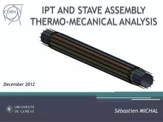
Stave+PetalProgramme • Collaboration of more than 25 institutes from 5 countries • Designed to minimise material • Early electrical systems tests needed to determine which mass-saving changes possible • Requirements of automated assembly built in from the start- Simplify build as much as possible!! • Minimize material in thermal management by shorting cooling path- Gluing module to a stave core with embedded pipes • Design aims to be low cost- Minimize specialist components! Petal Hybrid Glue Stave Module Glue No substrate or connectors ~ 1.2 meter Carbon fiber facing Bus cable Carbon honeycomb or foam Hybrids Coolant tube structure Readout IC’s A. Affolder – ACES 2011, 9th-11th March 2011, CERN
Electrical Test Vectors Single Module Frames • Frame with plug-ins for early testing of: • Serial Power Control (M-shunt, W-shunt, SPI) • Serial Power Protection (discrete or custom ASIC) • DC-DC convertors • Multi-drop AC-coupled LVDS clock/control (BCC) • Shielding/Grounding • 4 module devices for tests of: • System powering effects • DC-DC or Serial Power • Shielding/Grounding • Noise from AC-coupled MLVDS • DAQ development Stavelets • Simplified full length devices for specialized tests • Multi-drop AC coupled LVDS • Serial power protection Simplified full staves A. Affolder – ACES 2011, 9th-11th March 2011, CERN
Stave Module Noise Stave Module – Noise Signature • First modules were made with as thin as possible(<40 mm) glue layers between hybrid and sensor to reduce thermal paths and material • Saw increased noise due to coupling between hybrid shield and sensor • Modeled additional capacitance to hybrid in the same manner as the sensor backplane capacitance • Coupling different on inner/outer columns due to difference in hybrid overlap (9mm/15mm) Input Noise at 1fC AC Inner 604e 32 microns AC Outer 645e 15 microns DC Inner 580e 57 microns DC Outer 631e 25 microns A. Affolder – ACES 2011, 9th-11th March 2011, CERN
Stave Module Noise (2) Stave Module – Noise Signature • Increasing glue thickness to ~100 mm, decreases noise and increases uniformity with minimal to thermal performance (ASIC +1 C°) and module material (relative +1% to module’s X0) • Also much easier to mechanically maintain for large-scale production Input Noise at 1fC All tests performed using serial powering (hybrids at different potentials with one DC and one AC-coupled to sensor) AC Inner 143 microns 588e AC Outer 102 microns 599e Bad sensor channels DC Inner 589e 101 microns DC Outer 601e 94 microns A. Affolder – ACES 2011, 9th-11th March 2011, CERN
DC-DC Powered Module 740e Cu Tape wrapped around shield 733e Shows importance of early multi-module tests with new power schemes as this was a surprise. 675e 648e Hybrids shows increase of 70e- and 140 e- with respect to SP with painted copper shield • Painted shields were not effective against magnetic field coupling to power wire bonds – results in a uniform increase across all channels • Extra noise on Hybrid 62 is due to magnetic field contribution from both converters • Use of near field probe close to DCDC plug-ins confirmed this A. Affolder – ACES 2011, 9th-11th March 2011, CERN
DC-DC Power Module (2) 595e 603e Cu tape (50µm) Shield Larger system tests needed to determine optimal shield type and thickness Plated Cu Shield 595e 598e Noise comparable to SP with proper shielding A. Affolder – ACES 2011, 9th-11th March 2011, CERN
Stavelets Serial Power Protection PCBs or DC-DC Converters EOS Card power and power control data and hybrid communication BCC PCBs Bus Cable • Shortened Stave, built as electrical test-bed • Shielding,grounding, power, multi-drop LVDS • First Stavelet serial powered with “M” shunt • Power Protection Board (PPB) allows each SP hybrid to be bypassed under DCS control • Other powering options to be tested later • Using Basic Control Chip (BCC) • Generates 80MHz data clock from 40MHz BC clock • 160Mbit/s multiplexed data per hybrid • Readout using HSIO board from SLAC HSIO + interface A. Affolder – ACES 2011, 9th-11th March 2011, CERN
Serially Power Stavelet Noise Performance Custom Constant Current Source at 5A • Still more work to go, there is some indication that additional noise may be reduced by improving HV filtering and references between the two hybrids of each module • With current stave tapes, HV connected to sensor backplane after filtering on one of the modules • Used on hybrid M-shunt control circuit • Stavelet noise now approaching single module tests • Roughly ~20 e- higher • Biggest noise gain after improvements to external grounding/shielding • External LV & HV filter stages and shielded cables • Plans for filtering board for clock/command/data/NTC • Plans to extend tests with other SP plug-in controllers A. Affolder – ACES 2011, 9th-11th March 2011, CERN
Serial Powering Protection Test 0.5 W • Hybrid bypassing works as expected • P=VI=100 mV*5 A=0.5 W • Noise slightly lower with neighbour’s bypassed Constant Current Source at 5A, ODDS AND EVENS, Composite A. Affolder – ACES 2011, 9th-11th March 2011, CERN
Custom Constant Current Source Benchtop PS Current Source 100 mA 1 ms Current source is “stiffer” to ABCN25 current bump after trigger • Programmable current source has been prototyped • Designed for full-length stave, output up to 80V at 6A • Includes isolated USB interface and overvoltage protection/interlock A. Affolder – ACES 2011, 9th-11th March 2011, CERN
Serial Powering Stavelet Conclusions • All technology needed for SP has been prototyped and shown to work (and compatible with 130 nm CMOS) • Remaining concerns are locations of devices and number of units in a SP chain (concerned with both common mode build-up and failures) • Largest continuous current channeled through any one ASIC will be les than 200 mA • Largest power dissipation in SP control/protection ASICs is less than 50 mW • Hybrid voltage regulation will have several amps of reserve current handling • Have shown up to 10 A in a hybrid • Allows flexibility for set voltages/currents • Minimal impact on material budget (see later slide for details) • Last bit for ultimate noise performance still under study • But measured noise would yield 15:1 S/N at end of life • Will continue to work on noise to make sure all potential noise sources are understood A. Affolder – ACES 2011, 9th-11th March 2011, CERN
DC-DC Stavelet Plans • Bus tape modified to accept wire-bondable DC-DC converters • First parts available and tested, plan on mounting first module March/April • Plan on side-by-side comparison with SP stavelet at CERN (Building 180) DCDC Tape Detail of DC-DC stavelet bus tape + power tape A. Affolder – ACES 2011, 9th-11th March 2011, CERN
Serial Power Protection Studies • Mimics 8 hybrids + protection + regulators • Mimics clock dependent current loads • Studies power-up issues • Tests real-time circuits; can induce controlled “open circuits” • Tests 1-wire bypass circuits Voltage fluctuations when a real-time bypass fires M-shunt board “Serial power protection for ATLAS silicon strip staves”, D. Lynn, et al., Nucl. Instr. and Meth. A 633 (2011) 51-60 SPi board A. Affolder – ACES 2011, 9th-11th March 2011, CERN
Full-scale LVDS Test • Need to determine “maximal” chain for clock/command using AC-coupled multi-drop LVDS • Designed/manufactured the Buffer Controller Chip (BCC) in 250 nm IBM to allow multi-module testing in a serial power chain • Developed by SLAC/UCL/Cambridge/LBNL • Generates 80 MHz data clock and multiplexes data lines • Replaced in final chip set by Hybrid Controller Chip (HCC) • Chain of 24 BCC operated as a system on the full length bus • Sufficient amplitudes and short enough rise time for all positions for BCC to regenerate clocks correctly A. Affolder – ACES 2011, 9th-11th March 2011, CERN
Discussions with Designers • Early dialogue with ASIC and sensor designers has lead to modifications to increase manufacturability, reduce mass,…. • Increasing channel count to 256 per ASIC (4 FE bond rows) and moving clock/command to side of ASIC, halves needed number of ASICs and reduces needed metal layer in hybrid by 1 • Shrinks hybrids from 24 mm x 108 mm to 12 mm x 96 mm • This reduces the bare hybrid, solder, ASICs, SMDs, and epoxies by ~50% • Wire bond pad locations and chip size/placement set to allow for direct ASIC/sensor wire bonding • No pitch adaptors A. Affolder – ACES 2011, 9th-11th March 2011, CERN
Serial Power Protection ASIC Design of full SPP ASIC SPP 130 nm ASIC prototype (analogue control only) is in hand and will be tested shortly. Test board designed and ready for submission CMOS 8RF Module frame to use this plug-in is in production Prototype board suitable for both stand alone bench tests and use with module through power protection board connector. ( inches) A. Affolder – ACES 2011, 9th-11th March 2011, CERN
Bus Tape Shield Studies As the AL shield on the bus tape is the dominant source of tape’s material (~45%), studies are underway to determine how thin it can be made Solid Hatched A. Affolder – ACES 2011, 9th-11th March 2011, CERN • Use module mounted on frame with modified testing block to allow for a tape with a screened aggressor signal • Aggressor lines for single-ended and differential • Compare options for screen: • Full screen • No screen • 50% hatched screen 150/150 • 25% hatched. • Use HSIO to measure noise with w/o aggressor signals • Tests starting soon • Block, frame, tapes and module are all available
Shieldless Module Outer Column- 615 e- • Assembled a module with one shielded and one shieldless hybrid • Tested in SP chain with shieldless hybrid AC-coupled • Noise as expected with measured glue thicknesses and hybrid build • No high noise channels seen • Currently following up with double trigger tests Inner Column- 601 e- No reduction in electrical performance seen yet for going to shieldless hybrid. Reduces hybrid copper by ~30% and hybrid circuit production costs by ~30%. A. Affolder – ACES 2011, 9th-11th March 2011, CERN ATLAS Tracker Upgrade Week, 23rd-27th Feb 09
Estimates for Material from Power • Using currently understanding, the radiation length of material needed to service power has been estimated • Excludes extra bus tape and core material but this should be similar with both serial power and DC-DC convertors • Goal of less than 2% for a stave’s radiation length • Serial Power: 1 shunt per ABCN, 1 control and 1 protection ASIC per hybrid • Estimate 0.03% of a radiation length to stave from serial power • Mostly from extra needed hybrid area and AC-coupling capacitors • DC-DC: 1 converter per module • Estimate 0.23% of a radiation length to stave from converters • 33% from SMD capacitors, 27% PCB, 20% shield, 18% custom inductor • Studies are underway to reduce material further 13 mm 28 mm A. Affolder – ACES 2011, 9th-11th March 2011, CERN
Conclusion • Most mass-saving changes have gone through proof of principle testing • DC-DC powering shown to work with a module, serial powering for a stavelet • In the near-term, side-by-side testing of a DC-DC and serial powered stavelet planned at CERN Further electrical testing underway to take full advantage of the lower predicted power of the ABCn 130 nm A. Affolder – ACES 2011, 9th-11th March 2011, CERN
Scaling up the Serial Powered System The length of the SP chain and it’s reverence connections needs careful examination under dynamic conditions as we begin to scale up from one module towards a full stave. Simulation results Common Mode for Hybrid to EOS Signals The plot on the left shows a simulation result for a 12 hybrid SP loop when L1’s are being issued (modeled as a 20% increase in digital current for all ABC chips.) The plot shows the local hybrid reference vs EOS ground. This represents one source of common mode noise in the digital signaling between the EOS and Hybrid. These simulations show a significant the potential for a growing common mode signal as the length of the SP chain is increased. Hybrid Coupling to the End of Stave Potential (Shield) 100 pF (stray) 100 nF < 50mV < 50mV ~ 100mV ~ 150mV ~ 400mV ~ 100mV A. Affolder – ACES 2011, 9th-11th March 2011, CERN
Current Silicon Microstrip (SCT) MaterialCurrent Silicon Tracker(4 barrel strip layers)Module SupportMaterial Material Old ATLAS Barrel Module 12 ASIC of 300μm thickness for double-sided module read-out (ie just 6 read-out chips per side) New ATLAS sLHC-Tracker Module will need to have 80 ASICs in two hybrids for each side “The barrel modules of the ATLAS semiconductor tracker”. Nucl.Instrum.Meth.A568:642-671,2006. → Need to reduce material in future design concepts so design to get rid of hybrid substrate
Hybrids and their features • Hybrids are designed to come on a panel (8 per panel) – first steps towards industrialisation • Designed for machine placement and solder re-flow of passive components (capacitors, resistors, etc.) Mshunt control and Digital I/O • Panel dimensions: 300mm x 200mm • Hybrid dimensions: 24mm x 107.6mm • Hybrids + ASICs are electrically tested on panel • With final ASIC set (ABCnext, MCC, power), we could test all hybrids in the panel with one connection for data I/O and two for SP power chain • Finally, substrate-less hybrids are then picked out of panel with vacuum-jigging for module attachment Hybrid Power and sensor HV filtering (spec’d to 500V) 31 A. Affolder – ACES 2011, 9th-11th March 2011, CERN
SP Stave Architecture 24 hybrids in series, each at different potential wrt GND CLK & COM AC coupled at hybrid DATA AC coupled at end of stave Common GND at end of stave (DC-DC powered stave would look similar, apart from the absence of AC coupled IO) A. Affolder – ACES 2011, 9th-11th March 2011, CERN
Shunt Regulator Architectures • Hybrid with Shunt “W” • Use each ABCN’s integrated shunt regulator • Use each ABCN’s integrated shunt transistor(s) See “Serial power circuitry in the ABC-Next and FE-I4 chips” to be given this afternoon by W. Dabrowski • Hybrid with Shunt “M” • Use one external shunt regulator • Use each ABCN’s integrated shunt transistor(s) • Two (redundant) shunt transistors, 140mA each • Hybrid with SPi (or similar) • Use one external shunt regulator • Use one external power transistor See “The Serial Power Interface Chip”, to be given this afternoon by M. Trimpl Each option has its merits. All now available in silicon: final choice to be based upon test results.
HSIO Status • Wide collaboration of designer/developers (Cambridge, Freiburg, LBL, RAL, SLAC, UCL) • HSIO DAQ system and accessory cards have been distributed to ~20 sites • Software (SCTDAQ-based using C/C++ and root) and firmware packages are in use and well developed • Firmware Status: • Decided to split versions: • SVN head is bleeding-edge • Work plan in backup slide • SVN branch created for user firmware • uses September 2010 stavelet testing firmware plus EOS IDC16 capability • Also, we have some new developers: • SamerKilani (UCL) – I2C/1-wire interface • Tom Barber (Freiburg) – Fake event generator and histogramer • New features for software: • Histogramming • Trigger bunches • Double triggers (for readout noise injection) • Requires SVN head firmware Adapter Board EOS HSIO A. Affolder – ACES 2011, 9th-11th March 2011, CERN
G&S Improvements Aluminium baseplate under Stavelet Frame Tape to Frame Tape to Stavelet Core Screened HV Pairs EoS STARPOINT Screened LV Pairs SHIELD STARPOINT Litz between EoS and Shield grounds Chokes fitted to Control Ribbons A. Affolder – ACES 2011, 9th-11th March 2011, CERN Aluminium cover connected to baseplate with Cu Tape
ENC Differences A. Affolder – ACES 2011, 9th-11th March 2011, CERN