Z80 Overview
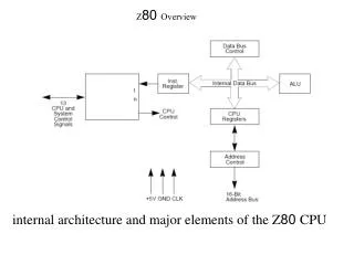
Z80 Overview. internal architecture and major elements of the Z80 CPU. Z80 Registers. All Z80 registers are implemented using static RAM. The registers include two sets of six general-purpose registers that may be used individually as 8-bit registers or in pairs as 16-bit registers.

Z80 Overview
E N D
Presentation Transcript
Z80 Overview internal architecture and major elements of the Z80 CPU
Z80 Registers All Z80 registers are implemented using static RAM. The registers include two sets of six general-purpose registers that may be used individually as 8-bit registers or in pairs as 16-bit registers There are also two sets of accumulator and flag registers and six special-purpose registers.
General Purpose Registers Two matched sets of general-purpose registers, each set containing six 8-bit registers, may be used individually as 8-bit registers or as 16-bit register pairs. One set is called BC, DE, and HL while the complementary set is called BC', DE', and HL'. At any one time, the programmer can select either set of registers to work through a single exchange command for the entire set. In systems that require fast interrupt response, one set of generalpurpose registers and an ACCUMULATOR/FLAG register may be reserved for handling this fast routine. One exchange command is executed to switch routines. This greatly reduces interrupt service time by eliminating the requirement for saving and retrieving register contents in the external stack during interrupt or subroutine processing. These general-purpose registers are used for a wide range of applications. They also simplify programing, specifically in ROM-based systems where little external read/write memory is available.
Accumulator and Flag Registers The CPU includes two independent 8-bit accumulators and associated 8-bit flag registers. The accumulator holds the results of 8-bit arithmetic or logical operations while the FLAG register indicates specific conditions for 8-bit or 1 16-bit operations, such as indicating whether or not the result of an operation is equal to zero. The programmer selects the accumulator and flag pair with a single exchange instruction so that it is possible to work with either pair.
Special-Purpose Registers Program Counter (PC) The program counter holds the 16-bit address of the current instruction being fetched from memory. The PC is automatically incremented after its contents have been transferred to the address lines. When a program jump occurs, the new value is automatically placed in the PC, overriding the incrementer.
Special-Purpose Registers Stack Pointer (SP) The stack pointer holds the 16-bit address of the current top of a stack located anywhere in external system RAM memory. The external stack memory is organized as a last-in first-out (LIFO) file. Data can be pushed onto the stack from specific CPU registers or popped off of the stack to specific CPU registers through the execution of PUSH and POP instructions. The data popped from the stack is always the last data pushed onto it. The stack allows simple implementation of multiple level interrupts, unlimited subroutine nesting and simplification of many types of data manipulation.
Special-Purpose Registers Two Index Registers (IX and IY) The two independent index registers hold a 16-bit base address that is used in indexed addressing modes. In this mode, an index register is used as a base to point to a region in memory from which data is to be stored or retrieved. An additional byte is included in indexed instructions to specify a displacement from this base. This displacement is specified as a two's complement signed integer. This mode of addressing greatly simplifies many types of programs, especially where tables of data are used.
Special-Purpose Registers Two Index Registers (IX and IY) The two independent index registers hold a 16-bit base address that is used in indexed addressing modes. In this mode, an index register is used as a base to point to a region in memory from which data is to be stored or retrieved. An additional byte is included in indexed instructions to specify a displacement from this base. This displacement is specified as a two's complement signed integer. This mode of addressing greatly simplifies many types of programs, especially where tables of data are used.
Interrupt Page Address Register (I) The Z80 CPU can be operated in a mode where an indirect call to any memory location can be achieved in response to an interrupt. The I register is used for this purpose and stores the high order eight bits of the indirect address while the interrupting device provides the lower eight bits of the address. This feature allows interrupt routines to be dynamically located anywhere in memory with minimal access time to the routine.
Memory Refresh Register (R) The Z80 CPU contains a memory refresh counter, enabling dynamic memories to be used with the same ease as static memories. Seven bits of this 8-bit register are automatically incremented after each instruction fetch. The eighth bit remains as programmed, resulting from an LD R, A instruction. The data in the refresh counter is sent out on the lower portion of the address bus along with a refresh control signal while the CPU is decoding and executing the fetched instruction. This mode of refresh is transparent to the programmer and does not slow the CPU operation. The programmer can load the R register for testing purposes, but this register is normally not used by the programmer. During refresh, the contents of the I register are placed on the upper eight bits of the address bus.
Arithmetic Logic Unit (ALU) The 8-bit arithmetic and logical instructions of the CPU are executed in the ALU. Internally, the ALU communicates with the registers and the external data bus by using the internal data bus. Functions performed by the ALU include: • Add /Subtract • • Logical AND, OR, XOR • • Compare • • Left or Right Shifts or Rotates (Arithmetic and Logical) • • Increment / Decrement • • Set / Reset Bit • • Test bit
PIN DESCRIPTION 40 21 Marker 1 20
Pin Functions BUS A15–A0 Address Bus (output, active High, tristate). A15-A0 form a 16-bit address bus. The Address Bus provides the address for memory data bus exchanges (up to 64 Kbytes) and for I/O device exchanges. D7–D0 Data Bus (input/output, active High, tristate). D7–D0 constitute an 8-bit bidirectional data bus, used for data exchanges with memory and I/O.
Pin Functions System Control IORQ Input/Output Request (output, active Low, tristate). IORQ indicates that the lower half of the address bus holds a valid I/O address for an I/O read or write operation. IORQ is also generated concurrently with M1 during an interrupt acknowledge cycle to indicate that an interrupt response vector can be placed on the data bus. M1 Machine Cycle One (output, active Low). M1, together with MREQ, indicates that the current machine cycle is the opcode fetch cycle of an instruction execution. M1 together with IORQ, indicates an interrupt acknowledge cycle.
Pin Functions System Control MREQ Memory Request (output, active Low, tristate). MREQ indicates that the address bus holds a valid address for a memory read of memory write operation. RD Read (output, active Low, tristate). RD indicates that the CPU wants to read data from memory or an I/O device. The addressed I/O device or memory should use this signal to gate data onto the CPU data bus. WR Write (output, active Low, tristate). WR indicates that the CPU data bus holds valid data to be stored at the addressed memory or I/O location.
Pin Functions System Control RFSH Refresh (output, active Low). RFSH, together with MREQ indicates that the lower seven bits of the system’s address bus can be used as a refresh address to the system’s dynamic memories.
Pin Functions CPU Control HALT HALT State (output, active Low). HALT indicates that the CPU has executed a HALT instruction and is waiting for either a non-maskable or a maskable interrupt (with the mask enabled) before operation can resume. During HALT, the CPU executes NOPs to maintain memory refresh. INT Interrupt Request (input, active Low). Interrupt Request is generated by I/O devices. The CPU honors a request at the end of the current instruction if the internal software-controlled interrupt enable flip-flop (IFF) is enabled. INT is normally wired-OR and requires an external pull-up for these applications.
Pin Functions CPU Control NMI Non-Maskable Interrupt (input, negative edge-triggered). NMI has a higher priority than INT. NMI is always recognized at the end of the current instruction, independent of the status of the interrupt enable flip-flop, and automatically forces the CPU to restart at location 0066H. RESET Reset (input, active Low). RESET initializes the CPU as follows: it resets the interrupt enable flip-flop, clears the PC and registers I and R, and sets the interrupt status to Mode 0. During reset time, the address and data bus go to a high-impedance state, and all control output signals go to the inactive state. Notice that RESET must be active for a minimum of three full clock cycles before the reset operation is complete.
Pin Functions CPU Control WAIT WAIT (input, active Low). WAIT communicates to the CPU that the addressed memory or I/O devices are not ready for a data transfer. The CPU continues to enter a WAIT state as long as this signal is active. Extended WAIT periods can prevent the CPU from properly refreshing dynamic memory.
Pin Functions CPU Bus Control BUSACK Bus Acknowledge (output, active Low). Bus Acknowledge indicates to the requesting device that the CPU address bus, data bus, and control signals MREQ, IORQ RD, and WR have entered their high-impedance states. The external circuitry can now control these lines. BUSREQ Bus Request (input, active Low). Bus Request has a higher priority than NMI and is always recognized at the end of the current machine cycle. BUSREQ forces the CPU address bus, data bus, and control signals MREQ IORQ, RD, and WR to go to a high-impedance state so that other devices can control these lines. BUSREQ is normally wired-OR and requires an external pull-up for these applications. Extended BUSREQ periods due to extensive DMA operations can prevent the CPU from properly refreshing dynamic RAMS.
Pin Functions CLK Clock (input). Single-phase MOS-level clock. +5V GND