Download
1 / 24
250 likes | 488 Views
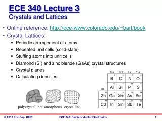
ECE 340 Lecture 3 Crystals and Lattices. Online reference : http://ece-www.colorado.edu/~ bart/book Crystal Lattices: Periodic arrangement of atoms Repeated unit cells (solid-state) Stuffing atoms into unit cells Diamond (Si) and zinc blende (GaAs) crystal structures Crystal planes

E N D
ECE 340 Lecture 3Crystals and Lattices • Online reference: http://ece-www.colorado.edu/~bart/book • Crystal Lattices: • Periodic arrangement of atoms • Repeated unit cells (solid-state) • Stuffing atoms into unit cells • Diamond (Si) and zinc blende (GaAs) crystal structures • Crystal planes • Calculating densities
Appendix III in your book (semiconductors): • Where crystalline semiconductors fit in (electrically):
The periodic lattice: • Stuffing atoms into unit cells: • How many atoms per unit cell? • Avogadro’s number: NA = # atoms / mole • Atomic mass: A = grams / mole • Atom counting in unit cell: atoms / cm3 • How do you calculate density?
The Silicon lattice: • Si atom: 14 electrons occupying lowest 3 energy levels: • 1s, 2s, 2p orbitals filled by 10 electrons • 3s, 3p orbitals filled by 4 electrons • Each Si atom has four neighbors • “Diamond lattice” • How many atoms per unit cell?
Zinc blende lattice (GaAs, AlAs, InP): • Two intercalated fcc lattices
Crystallographic planes and Si wafers • Si wafers usually cut along {100} plane with a notch or flat side to orient the wafer during fabrication
Where do (pure) Si wafers come from? • Read sections 1.3-1.4 in Streetman book • Take ECE 444 • Short answer: Image sources: Wikipedia
Graphite (~pencil lead) = parallel sheets of graphene • Carbon nanotube = rolled up sheet of graphene
The Bohr model of the (isolated) Si atom (N. Bohr, 1913): • Note: inner shell electrons screen outer shell electrons from the positive charge of the nucleus (outer less tightly bound) • Bohr model:
Quantum theory on two slides: 1) Key result of quantum mechanics (E. Schrödinger, 1926): • Particle/wave in a single (potential energy) box • Discrete, separated energy levels
2) Key result of wave mechanics (F. Bloch, 1928): • Plane wave in a periodic potential • Wave momentum k only unique up to 2π/a • Only certain electron energies allowed, but those can propagate unimpeded (theoretically), as long as lattice spacing is “perfectly” maintained‼! • But, resistance introduced by: __________ and __________
Energy levels when atoms are far apart: • Energy levels when atoms are close together (potentials interact): • Energy levels from discrete atoms to crystal lattice:
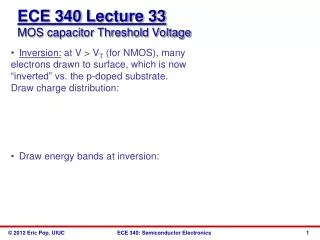
Energy states of Si atom expand into energy bands of Si lattice • Lower bands are filled with electrons, higher bands are empty in a semiconductor • The highest filled band = ___________ band • The lowest empty band = ___________ band • Insulators? • Metals?
Band structure explains why SiO2 (diamond, etc) is insulating, silicon is semiconducting, copper is a metal • For electrons to be accelerated in an electric field they must be able to move into new, unoccupied energy states. • Water bottle flow analogy (empty vs. full) • So, what is a hole then?
In devices we usually draw: • Simplified version of energy band model, indicating • Top edge of valence band (EV) • Bottom edge of conduction band (EC) • Their separation, i.e. band gap energy (EG)
ECE 340 Lecture 5Energy Bands, Temperature, Effective Mass • Typical semiconductor band gaps (EG) between 0-3 eV • GaAs → EG ≈ 1.42 eV • Si → EG ≈ 1.12 eV • Ge → EG ≈ 0.67 eV • … for more, see Appendix III in book • Insulator band gaps > 5 eV SiO2EG = 9 eV • Where are all electrons at T=0 K? • Do either insulators or semiconductors conduct at 0 K? • What about at T=300 K?
bond picture: (here 2-D) band picture: mechanical analogy:
How do band gaps vary with lattice size? (is there a trend?) • How do band gaps vary with temperature?
Short recap, so we are comfortable switching between: • Bond picture • Band picture vs. x • Band picture vs. k
Let’s combine energy bands vs. k and vs. x: • Note what is potential, kinetic, and total energy • Note which way energy of holes increases
Electrons (or holes) as moving particles: • Newton’s law still applies: F = m*a • Where m* = the “effective mass” of the particle, which includes all the complex influences of the crystal potential on the motion of the electron (or hole). • Acceleration? • For electrons: For holes: • Effective mass values? Fractions of m0. See Appendix III. • Sometimes depend on direction of motion in the crystal. • E.g. for electrons in Si: ml = 0.98m0, mt = 0.19m0 • Can also depend on particle location in the band (bottom, top, edge, “light” band vs. “heavy” band). • Values in Appendix III are given at the bottom of C-band for electrons, top of V-band for holes.
Q: What is the meaning of the energy band slope in the E-x band diagram picture?