Download
1 / 17
170 likes | 360 Views
Tight-Binding Modeling of Intermediate Valence Compound SmSe for Piezoelectronic Devices. Zhengping Jiang*, Yaohua Tan, Micheal Povolotskyi, Tillmann Kubis , Gerhard Klimeck (Purdue University) Marcelo Kuroda, Dennis Newns , Glenn Martyna (IBM)

E N D
Tight-Binding Modeling of Intermediate ValenceCompound SmSe for Piezoelectronic Devices Zhengping Jiang*, Yaohua Tan, Micheal Povolotskyi, TillmannKubis, Gerhard Klimeck (Purdue University) Marcelo Kuroda, Dennis Newns, Glenn Martyna (IBM) Timothy Boykin (The University of Alabama in Huntsville) *jiang32@purdue.edu
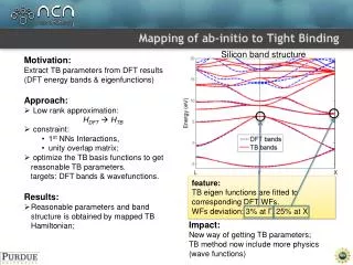
Outline • Motivation • Beyond Moore’s Law • Next Generation Switch • Piezoelectronic Transistor • Device Design • Working Principle • Metal Insulator Transition in SmSe • Tight Binding Parameterization • Summary
Beyond Moore’s Law Latest Generation FinFET 60mV/dec barrier still exist Technology drives device to scaling limit. Heat dissipation prevents any performance improvement through increasing clock frequency! Thinking Beyond Moore’s Law → Beyond Si FET
Next Switch Energy Filtering TFET Quantum tunneling instead of thermal emission Internal Voltage Step-up Internal Transduction Ferroelectronic FET & quantum capacitive device Spin fet & nano-electromechanical switch Lower voltage to flip spin then modulate barrier height Low Subthreshold Swing → Circumvent the Boltzmann distribution or break the direct voltage-barrier relation
Piezoelectronic Transistor (PET) Energy Filtering Internal Transduction Internal Voltage Step-up 3 Contacts 2 Channels PiezoResistive Material (e.g. SmSe) Current OUTPUT Pressure induced metal insulator transition Voltage INPUT RelaxorPiezoElectric Material (e.g. PMN-PT) Deformation due to E field Properties of PE and PR enable internal voltage step-up and internal transduction of acoustic and electrical signals.
Working principle Internal Voltage Step-up Internal Transduction Voltage applied on Gate – Common terminals: Deformation inside PE channel Electrical → Acoustic PR: insulator to metal transition Pressure on PR Gate Voltage Vg Current in PE channel Acoustic → Electrical Deformation Vg How does PET achieve SS<60mV/dec?
Mechanical and Electrical Features Large Area / Volume Ratio Between PE/PR Internal Transduction Hammer-Nail Effect Internal Voltage Step-up Small Deformation in PE → Large Strain in PR High response PE and big conductance change in PR SmSe High response Relaxor Piezoelectric Material Sound velocity in nanostructure → high speed Small Volume Change → Big Resistivity Change in PR Phys. Rev. Lett. 25, 1430 (1970) PET is capable of high performance and large scale integration! D. M. Newns, B. G. Elmegreen, X. H. Liu and G. J. Martyna, Advanced Materials (2012).
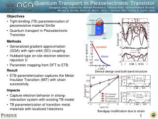
Metal-Insulator Transition in SmSe Conventional Ec f-electron band, New Ev Conventional Ev 5d 5d Eg = 0.45eV 4f Pressure 4f Insulating material Conducting material 4p 4p Scaling limit of PET determined by onset of tunneling. Quantum transport for MIT in tight-binding.
Methods 1. ab-initio calculation Ab-initio band structure Ei(k) Wave functions GGA + U 2. Determine TB model and fitting variables → Analytical formula for TB basis functions is Tesseral function, is to be parameterized • 3. Iteratively optimization • DFT Hamiltonian to TB Hamiltonian: basis transformation • Hab-initio HTB • Approximate HTB by two center integrals • Compare Ek with DFT and redo Step 3. Parameter refinement by simplex method → Target: Ek along high symmetry directions
Determine tight binding model DFT density of states: f-electron splitting due to strong correlation SmSe: DFT bandstructure • DFT decomposition: DOS into angular momentum • Se p-orbital: lower valence band • Sm d-orbital: conduction band • Sm f-orbital: top valence band • Splitting of f-orbital: covered through SO coupling Require TB model: sp3d5f7s* + SO
Strain effects on bandstructure of SmSe Bandstructure without strain Energy range most relevant to transport Energy range most relevant to transport Parameter fitted to band structure of hydrostatic strain and applied to clamped (uniaxial) strain with no modification. Bandgap is closing with strain in linear trend TB matches DFT trend!
Transport simulation PR layer is measured in thin film. Lateral length > Thickness Simulation is approximated by 1-D model. Periodic BC Extract 1-D simulation model with and without electric field.
Results Modeled imaginary band (b) and transmission (c) of SmSe thin film.
Summary • Piezoelectronic Transistor shows promising properties to overcome 60mV/dec limit. • Internal transduction • Internal “voltage” step-up • Metal-Insulator Transition in piezoresistive material is critical • Tight binding model could reproduce MIT from bandstructure effects • Second nearest neighbor TB model: sp3d5f7s*+SO • Strain model • Need modeling of Metal-SmSe interface and e-e scattering for f-electrons (work in progress)
Step: ab-initio calculation Ei(k), φi,k(r), Hab-initio Method Yl,m(θ,φ) Ab-initio band structure Ei(k) 2. Step:Define analytical formula for TB basis functionsn,l,m (r,,) = Rn,l(r)Yl,m(,)Yl,m(,) is Tesseral function, Rn,l(r) is to be parametrized Wave functions φi,k(r)
Method (continue) Step: Parameterize gettransform matrix U: ab-initio basis TB basis • 4. Step: • basis transformation (low rank approximation): • Hab-initio HTB • Approximate HTB by two center integrals; Iteratively optimize the TB results Step: Compare the TB results (band structure, wave functions) to ab-initio results; Measure the overlaps of basis functions; Step: Parameter refinement by simplex method → Target: Ek along high symmetry directions J. Slater & G.Koster PR. 94,1498(1964) A. Podolskiy & P. Vogl PRB 69, 233101 (2004)