Download
1 / 23
230 likes | 321 Views
Get prepared for group projects and exams in EECS 373 with tips on memory technology and exam review. Safety concerns and exam details covered, along with topics like memory architecture and landscape.

E N D
Memory technology and exam review EECS 373
Group projects • Meetings on Friday • Should have signed up. • If someone is going to be missing, let us know • Project ideas look fine • Safety is going to be a worry this semester • High speed things (helicopter blades, other spinney things) either need to be covered so can’t hurt anyone or done outside of lab with reasonable protection (safety glasses) in place. • Don’t think anyone has high-power draw issues… • Contacted some groups wrt their proposals • Mainly with things I want folks thinking about before Friday.
Exam • Exam is in lecture on Tuesday • Some folks will be in conference room in Beyster (CSE). • Where everyone will be placed will be sent in an e-mail over the weekend • Closed book closed notes • Can have a calculator • Can’t be a communication device (no cells) • May not have notes etc. in it. • Any needed document will be provided. • Old exams should give a reasonable idea about the exam format and coverage. • Exam Q&A Sunday at 3pm, room TBA
Topic talks (1/2) • 3/12: • DC motor with H-bridge • Ultrasonic distance sensors • 3/14: • Can Bus • VGA • 3/19: • Zigbee • Bluetooth • 3/21: • Interaction(s) with cameras • Kinect • 3/26: • Soldering • Gps • 3/28: • BAN • Flash • 4/2 • Radiation-hardened processors • Ethernet • USB • Error correcting hardware • 4/4: • Nvidia Low Power Mobile Tegra Processors • Parallel Processing • Analog-to-Digital Converters • Group 18
Topic talks (2/2) • To do: • Come to office hours as a group and discuss your topic with me about 2.5 weeks before the presentation. • About 1-1.5 weeks before the presentation’s scheduled date your group will give a preliminary presentation out-of-class (generally just to the instructor). Feedback will be provided on both technical and non-technical aspects of the talk. • About 0.5 weeks beforehand you’ll give a “final” practice version of your talk. • Then you’ll have about a 15 minute block in class to give the “real” presentation • I’ll have time on Doodle available for groups to do steps 2 and 3. • For step 4, come to office hours or grab me after class.
Memory • Memory Landscape • Memory Architecture • Non-volatile Memories • Volatile Memories
Basic categories of memory • Read-Only Memory (ROM) • Can only be read (accessed) • Cannot be written (modified) • Contents are often set before ROM is placed into the system • Random-Access Memory (RAM) • Can be read/written • Term used for historical reasons • Technically, ROMs are also random access • Volatile memory • Loses contents when power is lost • Often stores program state, stack, and heap • In desktop/server systems, also stores program executable • Non-volatile memory • Retains contents when power is lost • Used for boot code in almost every system notice how “wrong” this name is
Choosing the right memory requires balancing many tradeoffs • Volatility: need to retain state during power down? • Cost: wide range of absolute $ and $/bit costs • Organization: 64Kbx1 or 8Kbx8? • Interface • Serial or serial or parallel or parallel or parallel? • Synchronous or asynchronous? • Access times: critical for high-performance • Modify times: critical for write-intensive workloads • Erase process: at wire-line speed or 5 minutes in UV? • Erase granularity: word, page, sector, chip?
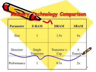
Internal organization of memory is usually an array Mem Cell Mem Cell Mem Cell Mem Cell word lines • Different memory • types (e.g. SRAM vs • DRAM) are • distinguished by the • technology used to • implement the • memory cell, e.g.: • SRAM: 6T • DRAM: 1T/1C Mem Cell Mem Cell Mem Cell Mem Cell Mem Cell Mem Cell Mem Cell Mem Cell From a chip design viewpoint, what should be the aspect ratio be? (# rows vs #cols)? Mem Cell Mem Cell Mem Cell Mem Cell From the user’s viewpoint, what should the aspect ratio be? bit lines
Outline • Memory Landscape • Memory Architecture • Non-volatile Memories • Volatile Memories
Physical (on-chip) memory configuration • Physical configurations are typically square • Square minimizes length of (word line + bit line) • Shorter length means • Shorter propagation time • Faster data access • Smaller trc (read cycle time) • Exercise: Assume n2 memory cells configured as • n-by-n square array. What is the worst case delay? • n2-by-1 rectangular. What is the worst case delay? • Exercise: Does wire length dominate access time? • Assume propagation speed on chip is 2/3 c (2x10^8 m/s) • Assume 1Mbit array is 1 cm x 1 cm
Logical (external) memory configuration • External configurations are tall and narrow • More address lines (12 to 20+, typically) • Fewer data lines (8 or 16, typically) • The narrower the configuration • The greater the pin efficiency • Adding one address pin cuts data pins in half • The easier the data bus routing • Many external configurations for given capacity • 64 Kb = 64K x 1 (16 A + 1 D = 17 pins) • 64 Kb = 32K x 2 (15 A + 2 D = 17 pins) • 64 Kb = 16K x 4 (14 A + 4 D = 18 pins) • 64 Kb = 8K x 8 (13 A + 8 D = 21 pins) • 64 Kb = 4K x 16 (12 A + 16 D = 28 pins) • 64 Kb = 2K x 32 (11 A + 32 D = 43 pins)
Supporting circuitry is needed to address memory cell and enable reads and writes Memory Array 16 bits (4 x 4) A0 Control signals Select chip Select memory cell Control read/write Map internal array to external configuration (4x4 16x1) A1 2:4 decoder A2 A3 4:1 mux/demux OE# Does mapping of specific address bits to the decoder or mux matter? (hint: think locality) CS# WE# D0
The memory-bus interface • Chip Select (CS#) • Enables device • Ignores all other inputs if CS# is not asserted • Write Enable (WE#) • Enables write tri-state buffer • Store D0 at specified address • Output Enable (OE#) • Enable read tri-state buffer • Drive D0 with value at specified address
Outline • Memory Landscape • Memory Architecture • Non-volatile Memories • Volatile Memories
EPROM • Erasable Programmable Read-Only Memory • Constructed from floating gate FETs • Charge trapped on the FG erases cell • High voltage (13V +) applied to the control gate • “Writes” the cell with a 0 • Allows FG charge to be dissipated • Erasing means changing form 0 1 • Uses UV light (not electrically!) • Electrons are trapped on a floating gate • Writing means changing from 1 0 • Erase unit is the whole device • Retains data for 10-20 years • Not used much these days • Costly because • Use of quartz window (UV transparent) • Use of ceramic package • PROM (or OTP) is same, just w/o window
Flash Memory • Electrically erasable (like EEPROM, unlike EPROM) • Used in many reprogrammable systems these days • Erase size is block (not word); can’t do byte modifications • Erase circuitry moved out of cells to periphery • Smaller size • Better density • Lower cost • Reads are like standard RAM • Can “write” bits/words (actually, change from 1 0) • Write cycle is O(microseconds) • Slower then RAM but faster than EEPROM • To (re)write from 0 1, must explicitly erase entire block • Erase is time consuming O(milliseconds to seconds) • Floating gate technology • Erase/write cycles are limited (10K to 100K, typically)
Outline • Memory Landscape • Memory Architecture • Non-volatile Memories • Volatile Memories
Static RAM • SRAMs are volatile • Basic cell • Bistable core • 4T: uses pullup resistors for M2, M4 • 6T: uses P-FET for M2, M4 • Access transistors • BL, BL# are provided to improve noise margin • 6T is typically used (but has poor density) • Fast access times O(10 ns) • Read/write speeds are symmetric • Read/write granularity is word
Dynamic RAM • Requires only 1T and 1C per cell • Outstanding density and low cost • Compare to the 6T’s per SRAM cell • Cost advantage to DRAM technology • Small charges involved relatively slow • Bit lines must be pre-charged to detect bits • Reads are destructive; internal writebacks needed • Generally need differential sense amplifiers • Values must be refreshed periodically • Prevents charge from leaking away • Complicates control circuitry slightly
Exam coverage (1/2) • ARM assembly • Coding; reading ISA entry for an instruction. • ABI: writing functions and calling them • Caller save, callee save, passing arguments, return values. • Misc: Linker, loader, Power-on-reset etc. • Memory mapped I/O and buses • Basic ideas of why and how • Simple bus; AHB; APB • Writing code to talk to MMIO devices
Exam coverage (2/2) • Interrupts • Basics of why and how • ARM interrupts • Enabling, disabling, pending, priority, preemption. • What happens on an interrupt in the hardware and how we return. • Timers • Capture; reference; prescalar; range; resolution. • Digital logic issues • 270 review (set-up/hold time) • Glitches and clock synchronization.