Capabilities Overview
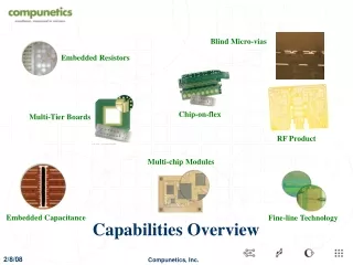
Multi-chip Modules. Fine-line Technology. Blind Micro-vias. Embedded Resistors. Chip-on-flex. Multi-Tier Boards. RF Product. Embedded Capacitance. Capabilities Overview. Agenda. Corporate Overview Compunetics, Inc. Company Profile Current Capabilities Technology Roadmap


Capabilities Overview
E N D
Presentation Transcript
Multi-chip Modules Fine-line Technology Blind Micro-vias Embedded Resistors Chip-on-flex Multi-Tier Boards RF Product Embedded Capacitance Capabilities Overview
Agenda • Corporate Overview • Compunetics, Inc. Company Profile • Current Capabilities • Technology Roadmap • Future Plans • Samples
Corporate Overview • 30+ Years Experience in Design, Development and Manufacture of Highly-sophisticated Electronic Systems • Telecommunications, Medical, Industrial, Transportation and Government Markets • Internal Control over Manufacturing • 330+ Employees
Corporate Overview Compunetix, Inc. Compunetics, Inc. Chorus Call, Inc. Instrumentation Systems Division Chorus Call, Inc. USA Communication Systems Division Printed Circuit Board Group Chorus Call International Switzerland Germany Italy India South Africa Greece Brazil Canada Australia Video Systems Division Federal Systems Division
PCB Layout & Design To Handle Customer Design Overflow And To Give Support To Customer’s Design Group Engineering Group Consisting Of 8 Engineers Dedicated To Managing / Fabricating Critical Or Technologically Challenging Projects Company Profile Compunetics, Inc. Manufacturing Sales / Marketing Quality Services Engineering Services Engineering Production Global Products Company Differentiators
Company Profile • SBA/FAR 19 Small Business • 38 Years Experience Producing Complex Interconnect Systems • Customers in Commercial, Education, Telecommunication, and Government Markets • Independent Internal R&D • ESOP • 2007 Revenues: $11.0 Million • 70+ Employees • 25+ Engineers and Professionals • ISO9001:2000 Registered and MIL Spec Certified
Company Profile Quality Certifications • ISO 9001:2000 Registered • UL Certified for Single / Double Sided and Multilayer Boards • ITAR Registered • MIL-P-55110 Certified for FR4, Polyimide • General Dynamics Land Systems Certified for Prototypes and Production • Hamilton Sundstrand Space Certification • JPL / NASA Flight Certified • General Dynamics UK Award For “Best Overall Business Performance 2004 / 2005”
Company Profile Types of Business • Prototypes, Quick Turn & Small To Medium Production • Military Spec PCBs • Backplanes • Rigid, Flex & Rigid/Flex (Class 2, 3 & Mil Spec) • High Layer Count – Up to 52 Layers, High Density PCBs • Independent Design/Drafting Group • Buried Passives • High Density Interconnects • Multi Chip Modules, Chip-On-Board • Engineering / Design Assistance
Company Profile Customer Base • Orbital • DRS • Northrop Grumman • Terumo • Raytheon • L3 Communications • Philips Medical • Maxtek • David Sarnoff • Bombardier • Kadflex • General Dynamics • Lockheed Martin • DoD / DoE • IBM • ITT / EDO • Intel • Tektronix • Land Systems • United Kingdom • AIS • ATP
Capabilities • Engineering Services • PCBs With 35 Micron Lines And Spaces • Multilayer PCBs 52 Layers + • Buried Resistors to 10%, Laser Trimmed to +/- 1% • Embedded Capacitors • Controlled Impedance to 2% • Blind and Buried Vias, Laser Micro Vias Including Stacked and Stepped Via Technology • 4 mil Mechanically Drilled Holes • Drafting and Design From Netlist (Gerber Generation) • Special Selective Plating • High Density Flex and Rigid Flex Circuits
Capabilities • Conductive Epoxy w/ Dupont CB100 • High Tolerance Laser Routing with Optical Alignment • Flex on Frames • Mechanical Routing with Optical Alignment • Controlled Depth Route to 2 mils • Panel Sizes to 28”x 26” • 3-Dimensional Plating • Sequential Build (Build-up Technology) • RF / Microwave Product • Heat Sink Boards • High Speed Laminates Including: Rogers, Taconic Arlon and High Speed FR4 (Isola, Nelco)
Technology Road Map Plating Aspect Ratio Current 12 Months 24 Months Production Engineering 9:1 12:1 10:1 13:1 11:1 14:1 PTH Tolerance (finished hole size) Current 12 Months 24 Months Production Engineering +/- 0.0030” +/- 0.0015” +/- 0.0025” +/- 0.0012” +/- 0.0020” +/- 0.0010”
Technology Road Map Soldermask And Screening Minimum Soldermask Web Current 12 Months 24 Months Production Engineering 0.0035” 0.0030” 0.0030” 0.0025” 0.0030” 0.0025” Minimum Soldermask Clearance Current 12 Months 24 Months Production Engineering 0.0030” 0.0025” 0.0025” 0.0020” 0.0025” 0.0020” Legend Min Height / Line Width Current 12 Months 24 Months 0.050” / 0.006” 0.040” / 0.005” 0.030” / 0.006” 0.035” / 0.005” 0.035” / 0.005” 0.030” / 0.004” Production Engineering
Technology Road Map *.0.062” thick board ** 0.125 thick board Mechanical Number of Layers Current 12 Months 24 Months Production Engineering 26 52 28 56 32 60 Smallest Mechanical Drilled Holes* Current 12 Months 24 Months Production Engineering 0.0060” 0.0040” 0.0060” 0.0040” 0.0050” 0.0030”
Technology Road Map Laser Drilled Microvias Minimum Hole to Capture Pad Current 12 Months 24 Months 0.004” / 0.008” 0.002” / 0.005” 0.005” / 0.009” 0.002” / 0.006” Production Engineering 0.006” / 0.010” 0.003” / 0.006” Aspect Ratio of Blind Microvia Current 12 Months 24 Months Production Engineering 0.5:1 0.7:1 0.6:1 0.8:1 0.7:1 1:1 Copper Filled Microvias Current 12 Months 24 Months Production Engineering No Evaluation No Yes Yes Yes Multi-Level Microvias (Stacked) Current 12 Months 24 Months Production Engineering No Yes Yes Yes Yes Yes
Technology Road Map Imaging And Mechanical Layer-to-Layer Registration Current 12 Months 24 Months Production Engineering +/- 0.0030” +/- 0.0020” +/- 0.0030” +/- 0.0020” +/- 0.0025” +/- 0.0014” Signal Pad Annular Ring Inners Current 12 Months 24 Months Production Engineering 0.0040” 0.0030” 0.0035” 0.0025” 0.0030” 0.0020” Plane Clearance Inners Current 12 Months 24 Months Production Engineering 0.016” 0.011” 0.014” 0.010” 0.012” 0.008” Copper Feature to Board Edge Current 12 Months 24 Months Production Engineering 0.0050” 0.0030” 0.0045” 0.0025” 0.0040” 0.0020”
Technology Road Map Imaging And Etching * Half Ounce Copper Trace / Space Outers * Current 12 Months 24 Months Production Engineering 0.0040” / 0.0040” 0.0015” / 0.0015” 0.0035” / 0.0035” 0.0012” / 0.0012” 0.0030” / 0.0035” 0.0010” / 0.0010” Trace / Space Inners * Current 12 Months 24 Months Production Engineering 0.0035” / 0.0035” 0.0015” / 0.0015” 0.0030” / 0.0030” 0.0012” / 0.0012” 0.0025” / 0.0030” 0.0010” / 0.0010” Trace Width Tol. Inners* Current 12 Months 24 Months Production Engineering +/- 0.0005” +/- 0.0003” +/- 0.0004” +/- 0.00025” +/- 0.0003” +/- 0.0002” Controlled Impedance Tolerance * Current 12 Months 24 Months Production Engineering +/- 10% +/- 2% +/- 7% +/- 2% +/- 5% +/- 2%
Future Plans • Investigating Laser Direct Imaging Equipment • Working With Dielectric Solutions On Reducing Fiber Weave Effect Using Proprietary Fiberglass Weave In PCB Materials • Evaluating Factory Relocation And Expansion • Sub-mil High Density Product • Multi-Layer LCP Packages • Investigating Large Panel Production Equipment
Samples Embedded Passives (Resistors) • A True Thin-Film, Nickel-Phosphorous (NiP) Alloy. • About 0.1 To 0.4 Microns Of The Alloy Is Electro-Deposited On To The Rough, Or Tooth Side Of Copper Foil During Manufacturing • Typical Tolerance Of 10 – 20% • Resistors Tested At Final Test And During Inner Layer OHMEGA-PLY LAMINATE copper resistive material (0.1-0.4 micron thick) dielectric substrate copper (EXAMPLE OF AVAILABLE CORE)
Cu Film Core Cu Copper clad laminate Double sided (power and ground) Dielectric is a Polyimide and BaTiO composite. Thickness of dielectric is key…thinner is better Samples Embedded Passives (Capacitors) • Bulk Capacitance Formed By Placing Power And Ground Layers Close Together • Thin Dielectrics Separate Power And Ground To Create Parallel Plate Capacitor C = keA/t Where: C = Capacitance e = Dielectric Constant of Material A = Board Area in Square Inches k = Permittivity of Free Space – Constant of 225 t = Dielectric Thickness in inches
Samples Embedded Passives (Capacitors) • Reduction In SMT Caps Needed On PCB • Closely Spaced Planes Have Lower Inherent Inductance Therefore Supply Current On A Very Short Time Scale Thus Damping Fluctuations Of Voltage At Device Input • Low Inductance Planes Reduces EMI • Initial Data Indicates That Surface Mounted Capacitance Can Be Effectively Replaced By Embedded Capacitance With Only A Small Fraction Of The Total Discrete Capacitance
Samples Embedded Passives (Capacitors) Products
Samples Embedded Passives (Capacitors) Application • Before Embedded Capacitance • 18 Layers • Blind vias: 1-2, 18-17 • Buried vias 2-17 • Over 2000 Caps • After Embedded Capacitance • 18 Layers • No Blind Vias • Buried vias 2-17 • Removed 800+ Caps
Samples Controlled Impedance Flex • Faster Signals with Faster Rise/Fall Times Require Controlled Impedance Flex Cables • In Order To Have Cable Flexible, Need To Etch Traces Near 3 mils (Larger Traces Require Thicker Dielectrics For Same Impedance, Making Board Less Flexible) • Controlled Impedance Flex • 8 Layers • Trace / Space – 3.0 / 3.0 • DuPont AP & LF Flex Material • Differential Controlled Impedance
Samples Rigid-Flex • Common Application To Add Reliability And/Or To Reduce Assembly Costs Through Removal Of Connectors And Cabling • More Common Due To Tight Spaces And Need For Increased Reliability In Products, Especially In Military • Military Avionics Rigid Flex • 8 Layers • 2 oz. Copper • Loose-leaf Design for Increase Flexibility • 3 Double Sided Flex Cores w/Coverlay • Military Specification
Samples Rigid-Flex • Satellite Systems • 12 Layers • Flight Certified Product • Polyimide / DuPont AP Flex • Immersion Gold • Military • 22 Layers • 6 Layer Loose-leaf Flex • Polyimide / DuPont AP Flex • HAL Finish
Samples High Speed – Mixed Material Boards • Need For Low Df/Dk Materials for Today’s Technology • Mix Low Df/Dk, High Cost Material with Higher Df/Dk Low Cost Material • Keep Critical Signals on/with Low Df/Dk Material • Some Materials can not be Mixed with Certain Other Materials • Mixed Material 10Gb Ethernet • 8 Layers • Blind Vias – 1-4 For Stub Control • Conductive Epoxy Filled Vias • Rogers 4003 / FR4 Material • Cavity Construction at Gold Fingers
FR4 Material (Glass Bundles) • Rogers 4000 (Ceramic Filled) Samples High Speed – Mixed Material Boards
Samples Heat Dissipation Boards • Smaller Spaces and Hotter Running Parts Require Design Consideration for Heat Dissipation • Need To Provide Thermal Path Away From Components • Several Design Changes Can be Made To Minimize Thermal Impact to Components • Place Heat Generating Part Near Heat Sink or Board Edge • Provide Thermal Path In Copper Including Using Edge Plating • Use Thermal Vias to Connect to Internal Planes or Heat Sink • Use of CB100 for Thermal Vias • Heat Sinks • Thinner Board Materials Place Component Closer To Heat Sink
Samples Heat Dissipation Boards • Heat Dissipation Board • 4 Layers • Thin Core FR4 • Conductive Epoxy • Heat Spreader Attached w/ Thermagon • HASL Finish
Samples RF Boards • Boards Typically Made on Teflon or Teflon Blend Products • Etching Tolerance of +/- .0003” • Several Areas of Tight Tolerance Routing +/- .002 (Requires Laser Routing w/Vision System • Some Designs Require Metal Backing • Most Require Wirebondable Gold
Samples RF Boards • Commercial RF • 2 Layers • Rogers 3003 • Laser Routed Slots • Trace Tolerance +/- .0003” • Wirebondable Gold • Military RF • 4 Layers • Rogers 6002, 4350, 4403 • Blind 1-2, 4-3; Buried 2-3 • Cavity 4 to 3 • Trace Tolerance +/- .0003” • Wirebondable Gold
Samples Laser Drilled Blind Micro-vias • Typically .004” to .006” Laser Drilled Hole From Layers 1 to 2 and/or From N to (N-1) • Dielectric Distance .003” to .004” • Aspect Ratios less than .50:1 • Material Typically RCC (Resin Coated Copper) or Flat Glass FR4 • Enables Pin Escaping Small Pitch BGAs or BGAs on Thick PCBs • Used to Conserve Routing Channels on Inner Layers • Enables Double Sided Assembly in Some Cases
Samples Laser Drilled Blind Micro-vias
Samples Chip On Flex (Direct Die Attach) • Chip On Flex • 2 Layers • Trace / Space – 2 / 2 • 2 mil Laser Drilled Vias • Wirebondable Gold • 2 mil Adhesiveless Pyralux
Samples Buried Resistors on Flex • Buried Resistor on Flex • 2 Layers • Ohmega Ply Resistor • Resistor Covered By Kapton • Immersion Silver Finish • 2 mil Adhesiveless Pyralux
Samples Laser Trimmed Embedded Resistors • Laser Trimmed Resistors • Resistor Laser Trimmed Under Measurement • Resistor Trimmed to +/- 1% • Final Resistor Tolerance +/- 3% • Application: High Speed Testing
Samples Copper Filled Micro-vias • Via-in-pad Provides Flat Pad Surface for BGA Attach • Flat Surface Optimal For Stacked Micro-vias • Need For Special Plating Chemistry • Need For Special Plating Equipment • Enables Pin Escaping High Pin Count .5 mm Pitch BGAs • Technology Under Development at Several US Shops
Samples Copper Filled Micro-vias Current Plating Technology
Samples Copper Filled Micro-vias • Test Vehicles Manufactured and Evaluated • Technology Approved for Production Using In-house Equipment • The Smaller The Hole, The More Flat the Plating • Plating of Close to 1:1 on Blind Microvias
Samples Copper Filled Micro-vias Stacked Micro-vias
Samples DuPont PF Material • All Polyimide Adhesive • Flex “prepreg” Without Acrylic • Lower Z-axis Expansion Without Acrylic • Increase Reliability • Much Lower Df (.02 vs. .004) • Product Withstands MIL-Spec Thermal Shock Testing • Product Still In Beta-Test at Several Shops Including Compunetics, Inc. • Evaluations On-going at Several Large OEMs
Samples DuPont PF Material • Multi-Layer Flex w/ PF Material • Multi-Layer Flex w/ LF Bondply
Samples Fine Line Technology (2 mil Trace/Space & Down) • Required for High Pin Count Fine Pitch BGA Routing (<= 0.5 mm Pitch) • Chip On Board / Chip On Flex • Used To Reduce Layer Count – More Tracks per Channel • Seen with Laser Drilled Micro-vias • Typically on Boards with Small Annular Rings • Can be Combined with Embedded Passives
Samples Fine Line Technology (2 mil Trace/Space & Down) • Multi-Level Chip Package • 6 Layer FR4 • 2 / 2 Trace / Space • Embedded Resistors for Termination • Multi-Level Cavity Construction • Wirebondable Gold • Fine Line Package • 1.5 / 1.5 (35 / 35 um) Trace / Space • Wirebondable Gold • 4 Layers FR4 • 31 mil Thick +/- 1 mil
Samples Laser Ablation Of Soldermask Problem • Tighter Pitch Parts Require Better Soldermask Registration • Conventional Mask Annular Rings Leave Insufficient Mask Dams • BGA Area Covered With Soldermask • YAG Laser Used To Remove Mask From BGA Pads • Mask Annular Ring Less Than 1 mil • Mask Dams Remain Aiding Assembly Solution