Download
1 / 54
540 likes | 548 Views
L13 11292016-L14 120616 ECE 5212 UConn F. Jain L14 Solar cells: Tandem, MEG, and QD Solar Cell. Notes page Slide# 9.1. Introduction and Overview-I 430 2-3 9.2 Solar Spectrum and Air Mass m 434 4-5 9.3 Absorption of Photons in Semiconductors, Materials, Concentrated Solar 435 6-10

E N D
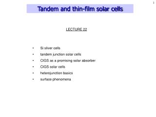
L13 11292016-L14 120616 ECE 5212 UConn F. Jain L14 Solar cells: Tandem, MEG, and QD Solar Cell Notes page Slide# 9.1. Introduction and Overview-I 430 2-3 9.2 Solar Spectrum and Air Mass m 434 4-5 9.3 Absorption of Photons in Semiconductors, Materials, Concentrated Solar 435 6-10 9. 4. Photovoltaic Effect: Voc, I-V equation, Vm-Im, Fill factor 440 11-15 9.5 Conversion Efficiency and Losses 448 16-18 9.6 Solar Cell Materials and Technologies: Generation I 450 19 9.7 Solved Examples 454 - 9.8.1 Solar Cell Design II: Design Solution AM m=1 458 20-28 9.8.2 Solar cell design for AM 0 469 - 9.9 Fabrication & Simulation of Solar Cells 473 - 9.10 Tandem Solar cell 475 29-33 9.11 Solar cell technology Part-III Tandem MEG, and QD Solar Cell 483 34-50 9.12 Problem set and solutions for solar design 51-52 9.13 Derivation of V-I equation of a n-p cell 513 -- 9.14 Solar summary equations 520 - Operating conditions and applications: Terrestrial applications Space application for satellites Electrical power output, conversion efficiency, cost/Watt-peak Cost of cells 25% Cost of fabricating modules/panels 25% Panel installation cost 50% 1 1
Photon absorption and creation of electron-hole pairs . Photons are generally absorbed in semiconductors when their energy is above the band gap Eg. This involves generation of electron-hole pairs (EHPs). An absorbed photon produces one EHP. Separation of electrons and holes before they recombine requires the presences of a barrier such as: p-n junction (homojunction or heterojunction) Schottky interface (MS, metal-semiconductor) or MIS (metal-thin insulator ~20A-semiconductor). Conversion efficiency ηc (Vm Im/Pin) The maximum power transfer (Vm, Im) is related to Fill factor FF is defined as (Vm Im)/(Voc Isc). It corresponds to fitting a maximum rectangle in the I-V characteristic. 2 2
Material Selection The maximum power that a cell can deliver is Isc *Voc. Short circuit current Isc depends on the band gap Eg; It is high for smaller energy gap semiconductors, Open circuit voltage Voc[~ (kT/q) * ln(Isc/Is)] depends on the ratio of Isc or IL and reverse saturation current Is. Since the reverse saturation current decreases as we increase the band gap Eg, it is low for higher energy gap materials. As a result the product of Isc *Voc peaks at Eg =1.4 eV. See Fig, 15. pp. 422; Figs. 34 and 35 below. 3 3
Solar cell summary equations p. 431-432 Air mass m is defined . Air mass m=2 or AM m=1.5 are taken as a typical average for the day. At m=2, we have 74mW/cm2 which produces ISC = 27mA for a cell sample of 1cm2. 4 4
Solar spectrum under m=0, m=1 m=0, 1300 W/m2 5
Absorption (Fig. 4, p. 434) . Absorption coefficient a depends on the material. Direct gap semiconductors have higher value near the energy gap Eg than indirect gap semiconductors. • Direct band-to-band with no phonon involvement. (2) b. Indirect band-to-band with phonon absorption or emission. (3) (phonon absorption) + (phonon emission) Fig. 5 shows photon flux or solar power or intensity I(x) decreases as the light propagates in the semiconductor. At m=2, we have 74mW/cm2 average power incident which produces ISC = 27mA for a cell of 1cm2. 6 6
Material selection for a solar cells: . The material selection depends on if the cell is to be used with concentrator or as is. Material could be single crystalline, polycrystalline, or amorphous. Generally the materials fall in two categories: (1) high efficiency (> 25%) cells, and (2) low efficiency (~10%) but inexpensive to fabricate cells. In the case of high efficiency cells, Olson and Friedman [1] have tabulated a number of material systems. These include: GaAs-GaInP, CuInSe/CdS, GaAs-CuInSe2 and CuInGaSe (CIGS) cells. Amorphous Si cells are used in portable electronics. Other popular materials include Si ribbon or polycrystalline Si. 7 7
Material selection for a solar cells: Competing solar panels . p-CdTe/n-CdS cells are η= 16.5 - 20% (First Solar). Doping of CdTe is due to vacancies. CdTe becomes n type with Te vacancies and p type with Cd vacancies. Deposition of CdTe is followed by processing including annealing at temperature T> 4000C in the presence of (CdCl2 + Oxygen) which gives optimal efficiency. CdTe films grown at low temperature becomes re-crystallized during this step. This improves the carrier life time which approaches tn~2ns. These cells give an open circuit voltage of Voc~810mV. Crystalline Si wafers: η= 20-25% Polycrystalline-Si wafers cells: η= 12.5-20%. (REF. M.A. Green, Progress in Photovoltiacs; Research and Appl., Vol 17, pp. 183-189, 2009.) aSi-on nanoSi-on glass η= 11-12%. Amorphous-Si cells are η= 10.1%. REF: M. Green et al, Progress in Photovoltaics: Research and Applications, 20, pp. 12-20, 2012 8 8
Concentrated Solar Photovoltaic (CSP) High efficiency (44-42% triple-junction e.g. Ge/GaAs/GaInP) solar cells are used with solar concentrators. Spire Corp. • Concentration (lenses/reflectors) is cost effective in module costs. • Olson and Friedman [1] suggest that a 1000 MW power plant using 1000X concentration would require less than 5000 m2 in cell area. Multi-junction and tandem cells are used in material system, which are expensive to fabricate. This way we increase their efficiency. Figure 1 shows a tandem cell that is built on p-GaAs substrate. It has two n-p junctions and one p+-n+ GaAs tunnel junction. The tunnel junction is between the TOP and BOTTOM solar cells. The tunnel junction provides the interface between the two cells. This enables a series connection between two n-p cells having the same series current. See Fig. 47, p. 467 or Fig. 1 page 430. Fig. 2. I-V Characteristics of a tandem cell. 9 9
Concentrated Solar Photovoltaic (CSP) Short circuit current increases and efficiency also increases. Fig. 24, p. 456 10 10
Photovoltaic effect: P-n junction under illumination with no load. P-n junction under equilibrium (27) 11 11
Photovoltaic effect: P-n junction under illumination with no load. P-n junction under illumination with load. 12 12
Equivalent Circuits: (27) 13 13
Open Circuit Conditions: V-I Equation : Equivalent Circuit Approach Generally, the behavior of a solar cell is modeled by the following equations. IL or ISC is the current under short circuit condition generated by absorption of photons. Open circuit voltage is obtained by putting I=0 in Eq. 27 an rearranging terms. (36) 14 14
Maximum Power Point (27) (36) Maximum power point (Vm, Im) is obtained using 40a) ,or (40b) Combining (40a, 40b) and Eq. (36) (48) 15 15
Fill Factor Fill Factor: FF: The fill factor is related to the shape of the V-I plot. (50) Conversion Efficiency The conversion efficiency is defined as the ratio of maximum electrical power output to the optical power incident. It is defined as (51) 16 16
Losses in Solar cells LOSSES: 1. Surface reflection: Calculate reflectivity R = Reflectivity of Si = R = Remedy: Design an antireflection coating using nr2 film. Let us design for 1.5eV photons. ,l =1,2 2. Long wavelength photons are not absorbed as when hv<Eg. the absorption coefficient is very small. 3. Excess photon energy loss : Calculation (see design set page 414): Photon energy above Eg is not used to generated electron-hole pairs (EHPs). This does not contribute to short circuit current ISC or IL. 17 17
Excess Energy Losses in Solar cells Compute these losses: AM1 plot above h > 1.1eV Regions are Triangle J, Trapezoid J, Trapezoid marked as #4, small rectangular regions #5 & #6. (triangle) J => Photon energy at = Photon energy at J = Average photon energy Excess photon energy not used in generating EHP= 3.21 – 1.1 = 2.11eV. Area of the triangle J = Excess energy not used in triangle J is = 18 18
6.6 Solar Cell Materials and Technologies: Generation I Flat Plate Arrays Silicon Based Single crystal wafers Ribbon Polycrystalline cast ingots Thin Films Cu2S/CdS polycrystalline Films GaAs thin layers on Sapphire ribbons Amorphous Si and Chalcogenide glasses films on steel Doped polyacetylene and other semi conducting polymers Arrays with Solar Concentrators Silicon wafers (30-50X) Gallium arsenide (50-200X) Graded heterostructures (50-5000X): thermal photovoltaic Tandem cells Multi Junction cells
Solar Design p. 456. Design a p+-n Si solar cell for terrestrial applications Air Mass m=1. Given: Material = n-Si, Resistivity = 10Ω-cm (see tables to find ND) Average power incident Pin for air mass m = 1 is 92.5 mW/cm2 (See attached Fig.25, Ref. Sze, Page 289) Specification desired: Fill factor ≥ 0.9 and power conversion efficiency ≥ 12%. • Evaluate the surface reflection loss. How would you design an antireflection coating to eliminate this loss (provide index and thickness of this coating). • Determine the optimum loading condition (Vmp, Imp), and compute fill factor for your cell and show that it is > 0.9 (change the ideality factor n if the fill factor is < 0.9). • Evaluate the other important losses and show that cell would be over 12% efficient. • Determine the doping concentrations and minimum thickness of n-region. Assume: Diffusion lengths (Ln, Lp) and minority lifetimes (τn, τp) as given in previous problems. Given that the p+ region is 0.25 micron thick and having a doping level NA = 1020 cm-3. IL or ISC: The photo generated current IL (or ISC) decreases as a function of the semiconductor band gap Eg. The open circuit voltage increases with Eg. 20 20
Design steps • Select a cell structure and absorber layer thickness and material. Find the photo-generated Isc • Design anti-reflection coating. • Select doping levels, find reverse saturation current Is and compute Voc, • Find Vmp, Imp or Vm, Im and fill factor FF. 21
Design steps cont. There are some ways to obtain a fill factor of 0.9. One-way is to reduce Is by increasing the doping of the substrate. The other way is to use a heterojunctions. Both results in high VOC. Reducing Is or Increasing VOC Increase the doping of the substrate. Let ND = 100*4*1014 = 4*1016 cm-3. We will keep NA for p+ = 1020 cm-3. Reduce losses due to: • Long wavelength (h < Eg of 1.1eV for Si) • Excess photon energy not used in generating electron-hole pairs. • Voltage factor (qVOC/Eg) • Fill Factor FF. • Current collection efficiency • (a measure of higher light generated current ISC) 22
Long wavelength photons not absorbed With reference to the figure, in area of region 1, 2 & 3, the solar power is: Region #1 68.4 W/m2 Region #2 72.69 W/m2 Region #3 35.77 W/m2 Total long wavelength (h < Eg of 1.1eV for Si) photons losses= 176.86 W/m2 23
Excess photon energy For the AM1 power plot above h > 1.1eV, we have 5 regions. • Regions are 1) Triangle J, 2)Trapezoid J, 3) Trapezoid marked #4, 4) Rectangle ’J, and 5) triangle ’. 24
Area of the J = Excess energy not used = Trapezoid J=> h at J => h at => Area = Rectangle ’J + ’ = 950*(0.84-0.51) + (0.84-0.51) * (1550-950)/2 = 412.5 W/m2 Excess energy lost = (412.5/1.953) * 0.843 = 178.05 W/m2 Trapezoid #4, Rectangle #5 & Rectangle #6 can be combined by a rectangle. = 500 * (0.84-1.1) = 130 W/m2 25
Excess energy per photon = have – Eg = 1.301 – 1.1 ~0.2eV Excess energy not used = Add all excess energy lost without being used as EHP = 101 + 178.05 + 19 298.05 W/m2 (iii) Voltage factor = (iv) Fill factor = 0.8 26
These four losses are plotted as follows Voltage factor 18% XXXX 14.4% 14.4% is reduced ~ 80% loss due collection efficiency (which impacts short circuit current ISC), we get 11.5%. Therefore, to design a cell at 12 the voltage factor needs to be improved by increasing Voc. 27
Absorber layer thickness (iv) Doping concentrations & minimum thickness of n-region. Pabs in n-Si = 925 – 176.86 = 748.14 W/m2 Pabs = Pin (1-e-(have)d) Where, d – thickness of n-region. hav = 1.9375eV, (at 1.9375eV) = 4*103 cm-1 In reality, d 100 – 150 m to absorb h Eg = 1.1eV. In reality, d 100 – 150 m to absorb h Eg = 1.1eV 28
Multi-junction cells using tunnel junction interface Here, the reverse saturation current density Js is expressed as: For the top cell: JsT= q [(DnT npoT/LnT) + (DpT pnoT/LpT)] (4A) For the bottom cell JsB= q [(DnB npoB/LnB) + (DpB pnoB/LpB)] (4B) 30
Short circuit current density in top and the bottom cells The short circuit current densities for the top and bottom cells are expressed in Eqs. 7 as: where I0(l) is the incident light intensity as a function of wavelength, h is Planck’s constant, c is velocity of light, aT(l) and aB(l) are the absorption coefficient in top and bottom layers, respectively, and tpT, tT and tpB are the thicknesses of p-absorbing layer (top cell), total thickness of top cell, and p-absorbing layer of the bottom cell, respectively. Also, k is the Boltzmann constant, and T the temperature. 31
Tandem solar cell Amorphous Si/ Crystalline Si Voltage Vs Current 33
Solar cells-iii Emerging new cell structures: Next we describe cells which have emerged during last 10 years. These include: 1. Sanyo’s HIT (heterojunction with intrinsic thin film) cell and amorphous Si window and crystalline Si cell 2. CdTe-CdS First Solar Corp. Cell 3. 4-5 junction tandem cells 4. Multiple exciton generation (MEG) cells 5. Intermediate Band Cell 6. Organic and polymer cells 7. Quantum dot and quantum wire cells. 8. Dye sensitized cells 34
Sanyo’s HIT Solar Cell using n-amorphous Si on p-crystalline Si and on glass substrates The HIT cells are surface textured on both sides of the wafer to eliminate reflections. Y. Tsunomura et al., Twenty two percent efficiency HIT solar cell”, Solar Energy Materials and Solar Cells, 93, pp. 670-673, 2009. Fig. 44 Sanyo’s Heterojunction with intrinsic thin film (HIT) cell. (a) cSi-aSi-TCO-Metal grid contact HIT n-aSiH/a-n+Si/p-type Si wafer. (b) Glass/TCO(bottom contact)/p-mcSi (30nm)/i-mcSi(1mm)/n-aSi (40nm)/ZnO/Ag/Al. TCO= Transparent conducting oxides serving as contact. tin oxide, indium tin oxide, ZnO. 35
CdTe thin film cells • Glass is deposited with fluorine doped tin oxide (FTO) and tin oxide at 550C, R=20 Ohm/sq • CdS layer by chemical bath deposition (CBD) using cadmium acetate, thiourea, ammonium acetate, ammonium hydroxide in a water bath at 92C • Deposit 4 micron CdTe at 660C using closed space sublimation (CSS) with a source plate of CdTe held at 660C for 2min. • RF sputter thin film of Cu:doped ZnTe. Ion mill 100nm of top ZnTe. • DC sputter titanium Ti thin contact. • Light is incident from glass substrate side. Rance et al , 14% efficient CdTe solar cells on ultra-thin glass substrates, Applied Physics Letter, 104, p. 143903, 2014. 36
Multi-junction Tandem cells Design Improve efficiency by: 1. Ge to absorb hv>0.67eV, --reduce long wavelength loss.2. Multiple energy gap absorbers--reduce excess energy loss 37
Excess energy loss: energy not utilized in electron-hole pair formation (Fig. 49) 38
Projected efficiencies Projected conversion efficiencies are for various 3rd generation cells: I. 66% Three-junction tandem cells 40-50% in some Multi-junction or Tandem Cells II 66% Quantum Dot solar cells using Multi-Exciton generation (MEG) III. Intermediate band (IB) devices. IV. Si nanowire solar cells. 39
Multiple excitons generation MEG: Alternate to harnessing excess energy loss Multiple exciton generation (MGE) phenomena and cells: Quantum Dot based solar cells When the photon energy hn is greater than the bandgap, the electron and hole generated have excess energy (hn-Eg) that is given up as phonons eventually heating up the lattice. That is, the energy of the hot carriers is lost. Excess energy can be recovered in following ways: (a)recover hot carriers before they thermalize (ref 2-4), and (b) hot carriers producing 2-4 electron hole pair via impact ionization or via multiple exciton generation. Multiple exciton generation (MEG, this is shown in QDs of PbSe, CdSe etc.) Impact Ionization 1 Photon creates 2 electron-hole pairs or exciton pairs. This is known as MEG. A new possible mechanism for MEG involves simultaneous creation of multiple excitons. No group has yet reported enhanced photo carriers in the external circuit. Quantum Yield ~ 300% when 3 excitons are formed. 40
One photon forms 3 excitons or 3 electron-hole pairs Fig. 51 Quantum yield is 300% if 3 excitons are formed 41
Intermediate band (IB) absorption to harness below gap photons Loss of below band gap and sub-band gap photons. Here an intermediate level is introduced by introducing a deep impurity level in the band gap. This is shown theoretically to be useful for single junction as well as tandem cells. Fig. 52 shows Intermediate band (due to impurity level or levels; supperlattice mini-bands, lone pair bands)in the middle of Conduction Band and Valence Band. Fig. 53. 3-D Analog of mini-bands found in superlattices 42
Types of QDot based Cells 1. Photoelectrodes composed of QD arrays. QDs such as InP (3-5nm dia) used to sensitize a TiO2 nanocrystalline film. 2.QDs dispersed in Organic/polymeric Semiconductors [i.e. in blend of electron and hole transporting polymers]. 3. Dye sensitized cells. 43
QD cells 44
QDot cells 45
Dye sensitized solar cells. Figure shows dye-sensitized solar cell57 using hybrid nanomaterials. 47
Solar modules The flowchart of Fig. 10(a) shows how energy conversion (solar cells) and storage (e.g. ultra-capacitors47-50) devices are used to implement alternate energy systems for various applications. Here, the middle block shows the interface circuits (such as micro-inverters27, solar tracking, and capacitor switching) depending on the application. Figure 48
Solar module cost Fig. 43. Module price as a function of power production. Fig. 45. Module cost /Wp in 2005. [Ref: A. Slaoui and R. Collins, p. 211, MRS Bull, March 07]The goal here is to obtain $1.82 to $1.2/Wp in 2010 and 2015, respectively. 49
Comparison of various technologies REF: M. Green et al, Progress in Photovoltaics: Research and Applications, 20, pp. 12-20, 2012 50