Metal-Semiconductor Contact
1.8k likes | 4.76k Views
Introduction Schottky Contact Ohmic Contact Interface Issues Practical Considerations Applications. Metal-Semiconductor Contact. MS Contacts: Introduction. Metal-semiconductor contacts can be ohmic or rectifying (allowing current flow only in one direction).

Metal-Semiconductor Contact
E N D
Presentation Transcript
Introduction Schottky Contact Ohmic Contact Interface Issues Practical Considerations Applications Metal-Semiconductor Contact
MS Contacts: Introduction • Metal-semiconductor contacts can be ohmic or rectifying (allowing current flow only in one direction). • Ohmic contacts do not limit current flowing in both directions (I-V curve may not need to be linearly related). • Rectifying contacts, generally called Schottky barrier diodes, limit current flowing in one direction. • Assumptions used: • (i) Metal and semiconductor in intimate contact in atomic scale with no other layers in between; • (ii) No inter-diffusion or inter-mixing of the metal and semiconductor; • (iii) No adsorbed impurities or surface charges at the interface. Reality?
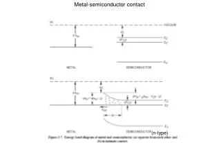
Schottky Contacts Consider an ideal metal-semiconductor (n-type) junction with metal work function larger than semiconductor work function. ФM>ФS (n-Si) E0 E0 q …… element charge E0 …… vacuum level …… electron affinity of silicon S …… work-function of silicon M …… work-function of metal q qs qM EC EFS EFM EV semiconductor (Si) metal How to draw eqm band diagram? Check handout & web learning aid!
Energy band diagram Thermal equilibrium condition (VA=0V) Schottky Contacts: Energy Band Diagram built-in potential: qVbi or Vo Barrier height electrons need to overcome from SC to M E0 E0 q qVo qs qB qM EFM EC EC EFS EFS EFM EV EV Bulk Silicon Metal x AFTER Contact BEFORE Contact barrier height: qФB Barrier height electrons need to overcome when flowing from M to SC
Schottky Contacts: Energy Band Diagram How depletion region forms W • Electrons with high energy move from Si to metal • Electrons accumulate at the surface of metal • Positive charged immobile ionized donors left behind in Si near interface depletion width W • Potential difference develops between the positively charged Si surface and metal opposes electron movement • Electron transfer continues until the contact potential is large enough to prevent further transfer • Equilibrium condition achieved Fermi levels aligned + + + Space charge region (also called depletion region) E0 E0 qM q qs EC EFM EFS EV Bulk Silicon Metal x NB: M and c are material constants which remain unchanged for the same material.
Barrier height and built-in potential =qФM-qФS 3 Schottky Contacts: Energy Band Diagram =qVo (built-in potential) 3 =q χ(electron affinity) 1 E0 1 E0 qVo=qФM-q ФS qM q qs 2 EFM EC Electrons on the SC side sees a barrier of M - S, reflected as a gradual lowering of the vacuum-energy level of thesemiconductor relative to the metal. EFS EV =qФB (barrier height) 2 Bulk Silicon Metal + = qФM 2 1 x qФB=qФM-qχ band bending occurs at interface (check: EF further away from EC means decreasing electron concentration)
Schottky Contact: Forward bias Forward bias condition (VA positive, semiconductor grounded) • contact potential is reduced from Vo–V • Electrons from semiconductor can drift across depletion region to metal and increasing V leads to a rapidly rising forward bias current, as an exponentially increasing number of electrons can surmount the surface barrier. See hand out and flash demo on website. http://courses.nus.edu.sg/course/elengv/ee3406/BandDiagram/index.html
Schottky Contact: Reverse Bias Reverse bias condition (VA is negative, semiconductor grounded) • reverse bias (-ve V) raises EFM aboveEFS, increases the barrier and blocks out the flow of electrons from semiconductor to metal • only a few electrons in the metal can surmount the energy barrier. - Barrier height remains unchanged, still equals to - reverse current remains constant with increasingly –ve bias.
Schottky Contact: Current Analysis The overall current of Schottky contact can be derived as following: where V is the voltage applied, I0 is the reverse saturation current and given by where A is the area of contact, Be is the effective Richardson constant and ФB is the potential energy barrier
Schottky Contact: Summary • Some discussions: • For many MS Schottky junctions, Be is 10-100 AK-2cm-2 typically. • In the early days, rectifying contacts were made by simply pressing a wire against the surface of a semiconductor. • SUMMARY • Schottky barrier diode is rectifying, with easy current flow in forward direction and little current in reverse direction. • Note that the forward current flow across a Schottky diode barrier is due to injection of majority carriers from S to M by thermionic emission (majority carrier device) • When external V is applied, the barrier is lowered by the Schottky effect.
E0 E0 q qM qs EC EFS EFM EV Ohmic Contact Consider an ideal metal-semiconductor (n-type) junction with metal work function smaller than semiconductor work function. ФM<ФS (n-Si) E0 E0 q qM qs EC EFM EFS EV AFTER Contact BEFORE Contact
E0 E0 q qM qs EC EFS EFM EV Ohmic Contact-thermal equilibrium Thermal Equilibrium (VA=0V) • After contact, electrons flow from metal into conduction band of semiconductor until thermal eqm is reached • accumulated electrons on semiconductor side prevent further electron movement from metal • potential drop of
Ohmic Contact- forward & reverse bias Reverse Bias (VA<0V) Forward Bias (VA>0V) • When bias is applied, practically all applied voltage drops across the higher resistance region which is the bulk neutral semiconductor. • Current is therefore determined by the resistance of the bulk, ie. measures property of device • no depletion region • accumulation of majority carriers near the semiconductor surface • low resistance to current flow • non-rectifying ohmic
Ohmic Contact Current-Voltage Characteristics • Some discussions: • Ohmic contacts have large current in both directions • Typically, the resistance is very small • Since the contact resistance is very small, the voltage will be dropped on the semiconductor Food for thought: Why does applied voltage result in displacement of Ef levels in Schottky band diagram (slides 53 & 54) but tilts Ef in ohmic band diagram (slide 59)?
MS Contacts – A Summary Check out hand out and flash demo. Verify by yourself
MS Contacts-Worked Eg • An n-type Si sample is doped with 1016 donors cm-3. The work function of metal M is 4.6eV. What contact is formed by the metal and the n-Si? Take effective density of states in conduction band, NC = 2.8 x 1025 m-3 for n-Si & electron affinity () of Si to be 4.01 eV. ФM>ФS (n-Si) so it forms a Schoktty contact
Schottky Contact: Quantitative Consideration Electrostatic variables in MS (n-type) contact under thermal equilibrium At semiconductor side, there is a depletion region where electrons are lacking (net +ve charge) However, no –ve acceptors to balance at metal side (unlike pn junction). Instead, a δ function of negative charge piles up at the MS interface at metal side. Therefore, depletion region is totally inside semiconductor (like pn junction with one side very heavily doped.
Schottky Contact: Quantitative Consideration Built-in potential DIY: prove this is same as ФM- ФS Charge Density
Schottky Contact: Quantitative Consideration Electric Field On semiconductor side, the electric field can be found through Poission’s equation Note limits Food for thought: What’s the electric field inside metal?
Schottky Contact: Quantitative Consideration Potential V=0 in bulk (ref) • Notes: • At thermal equilibrium, at x=0, V=-Vbi (built-in potential) • Depletion width is equivalent to the region on the semiconductor side where electrons are removed and +ve charged donors are left behind • When the applied voltage is VA, the effective potential at x=0 is VA-Vbi. This gives rise to the depletion width as Can you relate energy band diagram to this?
Interface Issues: Dangling Bonds • The consideration so far assumes the ideal system and that the semiconductors were infinite in extent. • All crystals terminate on surface surface atoms left with dangling bonds (bonds having only 1 electron) free electrons and molecules can be captured by dangling bonds (as shown above)
Interface Issues: Surface States • At the surface of a semiconductor, the crystal lattice is abruptly terminated perfect periodic potential of ideal single crystal lattice ends drastic irregularity introduces a large density of localized energy levels in the forbidden bandgap known as surface states (see fig on left) • Surface states can also be due to the presence of adsorbed gases, impurities at/near surface, changes in crystallographic structure or irregularities in the crystal. • They are also generally known as interface states as these effects are not restricted to the surface. Charges occur at metal-semiconductor interface due to incomplete bonds.
Interface Issues: Surface States Interface states have energy levels near the middle of the bandgap which act as efficient recombination centers. This has several possible effects: • Charge carriers filling these states can shift the energy levels up or down depending on the sign of these charges. This produces undesirable band bending for interfaces. • If the surface state density is high, these states (or traps) can capture charges. Charges can flow in and out of surface states producing only small shifts in the Fermi level relative to semiconductor bands. Hence surface charges tend to fix or to “pin” the equilibrium Fermi level at a specific energy within the bandgap. Example: a collection of interface states located 0.7-0.9 eV below ECpins the Fermi level at the surface of n-GaAs, and Schottky barrier height is determined from this pinning rather than the work function of metal.
In real life, a contact is seldom an atomically sharp discontinuity between semiconductor and metal, ie. not a sharp transition between semiconductor and metal regions. Typically, a thin interfacial layer (which is neither metal nor semiconductor) exists. Though electrons can tunnel through this thin layer, barrier height ФB to current transport through junctions is modified. Surface states also explain why most surface exposed to air are covered with a native oxide which is the result of dangling bonds capturing oxygen atoms. Interface Issues: Practical Issues
Ohmic Contact: Practical Consideration Approaches to achieve ohmic contact: • A low resistance contact to a semiconductor is obtained if the barrier height is small compared to kT. Carriers can flow over the barrier in either direction without much impediment. For example, ohmic contacts are obtained for ФM<ФS for an n-type semiconductor and ФM>ФS for a p-type semiconductor • In general, low resistance contact obtained when depletion region of the contact barrier is reduced in thickness (as shown in right fig) by heavy doping of semiconductor. Since a high field is present, field emission dominates current transport.
Ohmic Contact: Practical Consideration Degenerate Semiconductor with Ef inside conduction band • When doping level is low, only electrons energetic enough can surmount the energy barrier by thermionic emission (usually a small number of them) • As doping increases, the depletion width and width of barrier systemically decrease with increased semiconductor doping. When doping exceeds 1017 cm-3, significant tunneling can take place through the thin upper region of the barrier • When doping exceeds 1019 cm-3, the entire barrier becomes so narrow that even low energy electrons can tunnel through readily current flows freely
Ohmic Contact: Practical Consideration • Method to obtain ohmic contact: • evaporate metal on clean* surface, anneal to minimize contact resistance • usual contacts to Si include Ti, W, Mo (annealed to form respective silicides), Al (but not suitable if there are high temperature post processes). From previous section on surface states, we know that working in a clean environment is v important since impurities, interface states etc can modify contacts greatly. This is one of the reasons why microelectronic devices and circuits are fabricated in clean rooms.
Thermoelectric Cooler (I) When dc current flows through a contact between two dissimilar materials, heat is either released or absorbed in the contact region. • DC current is flowing from n-type semiconductor to metal through an ohmic contact. • Electrons flow from M to conduction band of semiconductor; current carried by electrons near EFM in the metal. • When electrons reach other end of contact region, their energy is EC+average KE (=3/2*kT) increase in average energy per electron in contact region electrons much absorb heat from environment through lattice vibrations to gain energy to drift through the junction.
Thermoelectric Cooler (II) Conversely, if current is from M to n-type S, electrons flow from conduction band of S to EFM in metal on passing through the contact. Since EFM is lower than EC, electrons lose energy through lattice vibration as heat Notes: • This thermoelectric effect occurs at a junction between any two dissimilar materials (not necessarily an ohmic contact) and called Peltier or thermoelectric effect. • (reverse process of Seebeck effect) • Do not confuse with Joule heating (=I2R) of S and M which arises from finite resistivity of material. This is due to conduction electrons losing energy gained from the applied field to lattice vibration when scattered by such vibrations.
Thermoelectric Cooler (III) • When dc current flows through semiconductor sample with metal contacts at its ends (as shown above), one end will always absorb heat and the other will release heat. • At the contact where heat is absorbed, the metal side (and the surroundings in contact with it) will be cooled and called the cold junction. • The other contact where heat is released will warm up the metal and surroundings and is called hot junction.
Thermoelectric Cooler (IV) • Current from n-type S to common metal electrode causes heat absorption which cools this junction and hence the metal. • Same current enters p-type S and causes heat absorption at this end, which cools the same metal electrode. • This end is in contact through a thin ceramic plate (electrical insulator but good thermal conductor) to a body to be cooled. • The other ends of the S are hot junctions which are connected to a large heat sink to remove heat, preventing heat conduction through S to cold junctions. Cross-section of typical thermoelectric cooler
Thermoelectric Cooler (V) A commercial example of thermoelectric cooler