Download
1 / 1
10 likes | 138 Views
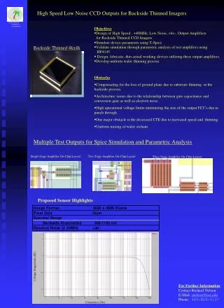
High Speed Low Noise CCD Outputs for Backside Thinned Imagers. Objectives Design of High Speed , +40MHz, Low Noise, <4e-, Output Amplifiers for Backside Thinned CCD Imagers Simulate device parameters using T-Spice Validate simulation through parametric analysis of test amplifiers using

E N D
High Speed Low Noise CCD Outputs for Backside Thinned Imagers • Objectives • Design of High Speed , +40MHz, Low Noise, <4e-, Output Amplifiers for Backside Thinned CCD Imagers • Simulate device parameters using T-Spice • Validate simulation through parametric analysis of test amplifiers using HP4145 • Design, fabricate, thin actual working devices utilizing these output amplifiers. • Develop uniform wafer thinning process. Backside Thinned 4kx4k • Obstacles • Compensating for the loss of ground plane due to substrate thinning in the backside process. • Architecture issues due to the relationship between gate capacitance and conversion gain as well as electron noise. • High operational voltage limits minimizing the size of the output FET’s due to punch through. • One major obstacle is the decreased CTE due to increased speed and thinning. • Uniform mixing of wafer etchant. Multiple Test Outputs for Spice Simulation and Parametric Analysis Single Stage Amplifier On-Chip Layout Two Stage Amplifier On-Chip Layout Three Stage Amplifier On-Chip Layout Proposed Sensor Highlights For Further Information: Contact Richard Nelson E-Mail: rnelson@uci.edu Phone: 949-824-4107