Understanding Active Matrix Displays for High-Resolution Output
Explore the complexities of Active Matrix Displays. Learn how TFT technology enables high resolutions by isolating individual pixels for better response and viewing angles. Dive into the principles of operation, addressing methods, and voltage variations crucial for effective display performance. Uncover the role of circuit scan lines, drain sources, and liquid crystal technologies in enhancing display quality. Discover the intricacies of addressing pixels in TFT technology and the necessity of a high voltage holding ratio for optimal performance.

Understanding Active Matrix Displays for High-Resolution Output
E N D
Presentation Transcript
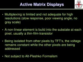
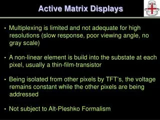
Active Matrix Displays • Multiplexing is limited and not adequate for high • resolutions (slow response, poor viewing angle, no • gray scale) • A non-linear element is build into the substate at each • pixel, usually a thin-film-transistor • Being isolated from other pixels by TFT’s, the voltage • remains constant while the other pixels are being • addressed • Not subject to Alt-Pleshko Formalism
Active Matrix Circuit Scan Line Drain Source Liquid Crystal
Principle of Operation-Active Matrix • One line at a time addressing • A positive voltage pulse (duration T/N, N # rows, T frame time) • is applied to the line turning on all TFT’s • The TFT’s act as switches allowing electrical changes to the • LC capacitors from the columns (data or source) • When addressing subsequent rows a negative voltage is • applied to the gate lines thereby turning off the transistors for • one frame time T, until ready to readdress it • For AC drives schemes (LCD’s) the polarity is alternated on the • data voltage
4 Basic Steps of TFT • At time 1, a positive voltage VG of duration T/N is applied to • gate to turn on TFT. The LC pixel (ITO) is changed to VON at • time 2 within T/N, due to the positive source voltage VSD=VON. • At time 2, the gate voltage VG becomes negative, turning off • the source voltage VSD from VON to –VON. During the time • period 2 and 3, of duration (N-1)/NT, the pixel voltage VP remains • about >0.9 VON as the LC capacitor is now isolated from data lines. • At time 3 (the next addressing time), the TFT is turned on again • by applying a positive gate voltage of duration T/N. The LC • capacitor now sees a negative source-to-drain voltage VSD=-VON. • The pixel electrode is discharged from VP=VON at time 3 to • VP=-VON within the time duration T/N. • At time 4, the TFT is turned off by the negative gate voltage, and • simultaneously the source voltage VSD changes from –VON to +VON.
TFT Addressing T/N T T VG Gate Voltage 0 time 4 3 1 2 VSD VON Source Drain Voltage time 0 VP Pixel Voltage time Notice that VP is not constant during the duration (n-1)T/N because of a slight leakage current of LC cell. LC materials must have a high voltage holding ratio (VHR) to minimize this.