ADS Design Guide
ADS Design Guide. Example (VCO). Example (VCO). Low-noise amplifier. TSMC 0.18 m CMOS process. Frequency: 2.4 GHz 3 dB B.W.: > 500 MHz DC consumption: < 20 mW, 1.8 V S 21 : > 15 dB S 11 /S 22 : < -10 dB N.F.: < 2 dB P1dB: > -5 dBm IIP3: > 5 dBm. Down-conversion Mixer.
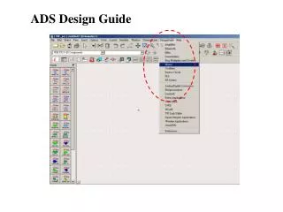

ADS Design Guide
E N D
Presentation Transcript
Low-noise amplifier TSMC 0.18 m CMOS process Frequency: 2.4 GHz 3 dB B.W.: > 500 MHz DC consumption: < 20 mW, 1.8 V S21: > 15 dB S11/S22: < -10 dB N.F.: < 2 dB P1dB: > -5 dBm IIP3: > 5 dBm
Down-conversion Mixer TSMC 0.18 m CMOS process fRF: 2.4 GHz, fLO: 2.3 GHz, fIF: 100 MHz DC consumption: < 10 mW, 1.8 V Conversion gain: > 5 dB @ LO power=-3 dBm S11/S22: < -10 dB Port-to-port isolation: > 20 dB P1dB: > -5 dBm IIP3: > 5 dBm
LC voltage-controlled oscillator TSMC 0.18 m CMOS process Center frequency: 2.4 GHz DC consumption: < 30 mW, 1.8 V, with output buffer Tuning range: > 1 GHz Output power: > 0 dBm Harmonic suppression: > 15 dBc Phase noise: < -120 dBc/Hz@1 MHz
RF switch circuit WIN 0.15 m pHEMT process Single-pole-double-throw Frequency: 1~5 GHz Insertion loss: < 1.5 dB S11/S22: < -10 dB Isolation: > 25 dB P1dB: > 25 dBm IIP3: > 35 dBm Harmonic suppression: > 30 dBc


![Remove Ads by TermTrident [Removal Guide]](https://cdn4.slideserve.com/7194315/slide1-dt.jpg)