Download

1 / 28
280 likes | 411 Views
EE5342 – Semiconductor Device Modeling and Characterization Lecture 11 - Spring 2005. Professor Ronald L. Carter ronc@uta.edu http://www.uta.edu/ronc/. Project 1. Some initial data and assignments for Project 1 are posted at http://www.uta.edu/ronc/5342/projects/Project_1/IVdata.xls and

E N D
EE5342 – Semiconductor Device Modeling and CharacterizationLecture 11 - Spring 2005 Professor Ronald L. Carter ronc@uta.edu http://www.uta.edu/ronc/
Project 1 • Some initial data and assignments for Project 1 are posted at http://www.uta.edu/ronc/5342/projects/Project_1/IVdata.xlsand http://www.uta.edu/ronc/5342/projects/Project_1/CVdata.xls
Additional Project 1 Actions • Develop the best least squares* static model (IS, N, ISR, NR, RS) for operating the diode in the range 700mV < vext < 1000mV *i.e. minimize • Repeat for the range 300mV to 1V
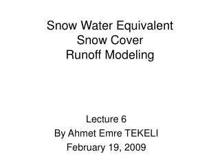
Id,ext (A) Vd,ext (V) SPICE Diode Static I-V
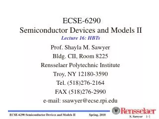
CJ0 = 1E-12 VJ = 0.75 M = 0.5 TT = 1E-9 100 pA 1 nA 10 nA 100 nA Re{Z} (Ohms) 1 mA (2pTT)-1 10 mA 100 mA 1 mA 10 mA Frequency (Hz) SPICE Diode Re{Z}
SPICE Diode Temp. Pars.1 PARAMETER definition and units default value XTI IS temperature exponent 3.0 TIKF ikf temperature coefficient (linear) °C -1 0.0 TRS1 rs temperature coefficient (linear) °C -1 0.0 TRS2 rs temperature coefficient (quadratic) °C -2 0.0 TBV1 bv temperature coefficient (linear) °C -1 0.0 TBV2 bv temperature coefficient (quadratic) °C -2 0.0 T_ABS absolute temperature °C T_MEASURED measured temperature °C T_REL_GLOBAL relative to current temperature °C T_REL_LOCAL Relative to AKO model temperature °C
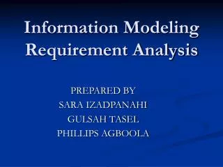
348K < TNOM < 300K 80 mW Rth = 600 K/W, RS = 1 W 70 mW Rth = 0 K/W , RS = 0.32 W 60 mW 50 mW Id (A) 40 mW 30 mW 20 mW 10 mW Vd,ext = Vd + Id*RS Self-Heating Effects
Self-Heating Effects • SPICE models the IS, etc. the same for all power dissipations. • The effect of diode self-heating is to increase the current at all voltages. • In this case, an Rth of 600K/W gave nearly the same simulation as re-setting RS from 1 Ohm to 0.32 Ohm. • The diode Tj is different at all curr.
PiN Diode • PiN: Na >> Nint (= N-) & Nint << Nd • Wi = Intrinsic region (metall.) width • Em,P-T = Peak field mag. when xn = Wi • Vbi = fi = Vtln(NaNd/ni2) • Vbi,int = fi,int = Vtln(NaNint/ni2) • VHL = Vtln(Nd/Nint), the offset at N+N- • Vbi = Vbi,int + VHL • VPT = applied voltage when xn = Wi
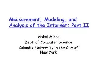
dx’n dx’p x’n -x’p Normalized Field, E/Em,P-T Normalized Position, x’ = x/Wi PiN Diode Depletion Fields
Estimating Junction Capacitance Parameters • Following L29 – EE 5340 Fall 2003 • If CJ = CJO {1 – Va/VJ}-M • Define y {d[ln(CJ)]/dV}-1 • A plot of y = yi vs. Va = vi has slope = -1/M, and intercept = VJ/MF
Derivatives Defined The central derivative is defined as (following Lecture 14 and 11) yi,Central = (vi+1 – vi-1)/(lnCi+1 – lnCi-1), with vi = (vi+1 + vi-1)/2 Equation A1.1 The Forward derivative (as applied to the theory in L11 and L14) is defined in this case as yi,Forward = (vi+1 – vi)/(lnCi+1 – lnCi), with vi,eff = (vi+1 + vi-1)/2 Equation A1.2
Data calculations Table A1.1. Calculations of yi and vi for the Central and Forward derivatives for the data in Table 1. The yi and vi are defined in Equations A1.1 and A1.2.
y vs. Va plots Figure A1.3. The yi and vi values from the theory in L11 and L14 with associa-ted trend lines and slope, intercept and R^2 values.
It is clear the Central derivative gives the more reliable data as the R^2 value is larger. M is the reciprocal of the magnitude of the slope obtained by a least squares fit (linear) plot of yi vs. Vi VJ is the horizontal axis intercept (computed as the vertical axis intercept divided by the slope) Cj0 is the vertical axis intercept of a least squares fit of Cj-1/M vs. V (must use the value of V for which the Cj was computed). The computations will be shown later. The results of plotting Cj-1/M vs. V for the M value quoted below are shown in Figure A1.4 Comments on thedata interpretation
M = 1/2.551 = 0.392 (the data were generated using M = 0.389, thus we have a 0.77% error). VJ = yi(vi=0)/slope =1.6326/2.551 = 0.640 (the data were generated using fi = 0.648, thus we have a 1.24% error). Cj0 = 1.539E30^-.392 = 1.467 pF (the data were generated using Cj0 = 1.68 pF, thus we have a 12.6% error) Calculating theparameters
Linearized C-V plot Figure A1.4. A plot of the data for Cj^-1/M vs. Va using the M value determined for this data (M = 0.392).
Additional Project 1 Actions • What forward voltage range actually fits the standard CV model? Hint: this will be for Va > VPT. • What auxiliary circuit would you add in order to model the diode for operation at Va < VPT?
2/24 and 3/1 class • Project workday on 2/24 – no class • Meet on 3/1 in 212 ELB • Be sure you have a gamma account and can access iccap. If problems, send questions to helpdesk@uta.edu • We will start using iccap and have a demonstration. • Check project web page for updates
References 1 OrCAD PSpice A/D Manual, Version 9.1, November, 1999, OrCAD, Inc. 2 Semiconductor Device Modeling with SPICE, 2nd ed., by Massobrio and Antognetti, McGraw Hill, NY, 1993.