8086 Pin Function
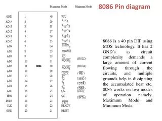
8086 Pin Function. By: Mahendra B. Salunke SITS, Narhe. Pin Diagram. Pin Functions. Out of 40 pins, 32 pins are having same function in minimum or maximum mode, And remaining 8 pins are having different functions in minimum and maximum mode.

8086 Pin Function
E N D
Presentation Transcript
8086 Pin Function By: Mahendra B. Salunke SITS, Narhe
Pin Functions • Out of 40 pins, 32 pins are having same function in minimum or maximum mode, • And remaining 8 pins are having different functions in minimum and maximum mode. • Following are the pins which are having same functions
Symbol: AD15 - AD0, Pin No. 39, 2-16 Type: I/O • ADDRESS DATA BUS: time multiplexed memory/IO address (T1), and data (T2, T3, TW, T4) bus. • These lines are active HIGH and float to 3-state OFF during interrupt acknowledge and local bus ``hold acknowledge''.
Symbol: A19/S6, A18/S5, A17/S4, A16/S3Pin No: 35 - 38 Type: O • Address/ Status lines • During T1: Address and then during T2, T3, Tw, T4 Status • S5: IF flag condition and S6: LOW
Symbol: BHE#/S7Pin No.: 34Type: O • Bus High Enable / Status:
Symbol: RD#Pin No.: 32Type: O • Read: RD# is active LOW during read cycle in T2, T3 and Tw clocks and indicates that processor is performing memory or I/O read
Symbol: READYPin No.: 22Type: I • Ready signal is received from memory or I/O devices to indicate the completion of data transfer • Synchronized by 8284 clock generator
Symbol: INTRPin No.: 18Type: I • Interrupt Request: Level triggered input received from interrupting device • Sampled during last clock of each instruction cycle • A subroutine is vectored through IVT if interrupt enable flag (IF) is SET
Symbol: TEST#Pin No.: 23Type: I • Test: Input is examined by the ‘wait’ instruction, if TEST# is LOW processor will continue execution otherwise wait in an idle state.
Symbol: NMIPin No.: 17Type: I • Non Maskable Interrupt: Edge triggered input causes a TYPE 2 interrupt. • Not maskable internally by software.
Symbol: RESETPin No.: 21Type: I • Reset: Input causes the processor to immediately terminate its present activity • Must be HIGH for at least 4 clock cycles
Symbol: CLKPin No.: 19Type: I • Clock: provides the basic timing for the processor and bus controller. • It is asymmetric with a 33% duty cycle to provide optimized internal timing.
Symbol: VccPin No.: 40 • Vcc: +5V power supply pin.
Symbol: GNDPin No.: 1, 20 • GROUND
Symbol: MN/MX#Pin No.: 33Type: I • MINIMUM/MAXIMUM: indicates what mode the processor is to operate in. • HIGH indicates minimum mode (Single processor system) • LOW indicates maximum mode (Multi-processor system)
Pins having different functions in maximum mode • Pin number 24 to 31 is having different functions in maximum mode which is explained below
Symbol: S2#, S1#, S0# Pin No.: 26-28Type: O • Status: active during T4, T1, and T2 and is returned to the passive state (1, 1, 1) during T3 or during TW when READY is HIGH • Used by the 8288 Bus Controller to generate all memory and I/O access control signals
Symbol: RQ#/GT0#, RQ#/GT1#Pin No.: 30, 31Type: I/O • Request/Grant: Pins are used by other local bus masters to force the processor to release the local bus at the end of the processor's current bus cycle. • RQ/GT0# is having higher priority than RQ/GT1#
Symbol: LOCK# Pin No.: 29Type: O • LOCK: output indicates that other system bus masters are not to gain control of the system bus while LOCK is active LOW. • Activated by the ``LOCK'' prefix instruction and remains active until the completion of the next instruction.
Symbol: QS1, QS0 Pin No.: 24, 25Type: O • Queue Status: The queue status is valid during the CLK cycle after which the queue operation is performed.
Pins having different functions in minimum mode • Pin number 24 to 31 is having different functions in minimum mode which is explained below
Symbol: M/IO#Pin No.: 28Type: O • Status Line: used to distinguish a memory access from an I/O access • HIGH for memory operation and • LOW for I/O operations
Symbol: WR#Pin No.: 29Type: O • Write: indicates that the processor is performing a write memory or write I/O cycle
Symbol: INTA#Pin No.: 24Type: O • Interrupt Acknowledgement: used as a read strobe for interrupt acknowledge cycles • Active LOW during T2, T3 and TW of each interrupt acknowledge cycle.
Symbol: ALEPin No.: 25Type: O • Address Latch Enable: It is a HIGH pulse active during T1 of any bus cycle • Provided by the processor to latch the address into the 8282/8283 address latch.
Symbol: DT/R#Pin No.: 27Type: O • Data Transmit/Receive: used to control the direction of data flow through the transceiver
Symbol: DEN#Pin No.: 26Type: O • Data Enable: provided as an output enable for the 8286/8287 in a minimum system which uses the transceiver
Symbol: HOLD, HLDAPin No.: 31, 30Type: I, O • Hold: indicates that another master is requesting a local bus ``hold.'‘ • The processor receiving the ``hold'' request will issue HLDA (HIGH) as an acknowledgement
Web: www.salunke.webs.com E-mail: msalunke@gmail.com Happy Learning

![8086 [2]](https://cdn1.slideserve.com/2457127/8086-2-dt.jpg)