Download

1 / 34
650 likes | 2.02k Views
Gursharan Singh Tatla professorgstatla@gmail.com. PIN DIAGRAM OF 8086. Gursharan Singh Tatla. Intel 8086. Intel 8086 was launched in 1978. It was the first 16-bit microprocessor. This microprocessor had major improvement over the execution speed of 8085.

E N D
Gursharan Singh Tatla professorgstatla@gmail.com PIN DIAGRAM OF 8086 www.eazynotes.com Gursharan Singh Tatla
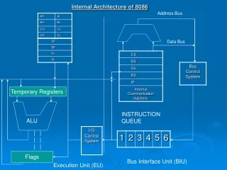
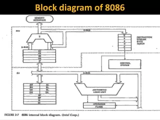
Intel 8086 • Intel 8086 was launched in 1978. • It was the first 16-bit microprocessor. • This microprocessor had major improvement over the execution speed of 8085. • It is available as 40-pin Dual-Inline-Package (DIP). www.eazynotes.com Gursharan Singh Tatla
Intel 8086 • It is available in three versions: • 8086 (5 MHz) • 8086-2 (8 MHz) • 8086-1 (10 MHz) • It consists of 29,000 transistors. www.eazynotes.com Gursharan Singh Tatla
Intel 8086 • It has a 16 line data bus. • And 20 line address bus. • It could address up to 1 MB of memory. • It has more than 20,000 instructions. • It supports multiplication and division. www.eazynotes.com Gursharan Singh Tatla
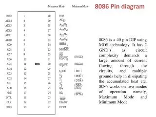
Pin Diagram of Intel 8086 www.eazynotes.com Gursharan Singh Tatla
AD0 – AD15Pin 16-2, 39 (Bi-directional) • These lines are multiplexed bi-directional address/data bus. • During T1, they carry lower order 16-bit address. • In the remaining clock cycles, they carry 16-bit data. • AD0-AD7 carry lower order byte of data. • AD8-AD15 carry higher order byte of data. www.eazynotes.com Gursharan Singh Tatla
A19/S6, A18/S5, A17/S4, A16/S3Pin 35-38 (Unidirectional) • These lines are multiplexed unidirectional address and status bus. • During T1, they carry higher order 4-bit address. • In the remaining clock cycles, they carry status signals. www.eazynotes.com Gursharan Singh Tatla
BHE / S7Pin 34 (Output) • BHE stands for Bus High Enable. • BHE signal is used to indicate the transfer of data over higher order data bus (D8 – D15). • 8-bit I/O devices use this signal. • It is multiplexed with status pin S7. www.eazynotes.com Gursharan Singh Tatla
RD (Read)Pin 32 (Output) • It is a read signal used for read operation. • It is an output signal. • It is an active low signal. www.eazynotes.com Gursharan Singh Tatla
READYPin 22 (Input) • This is an acknowledgement signal from slower I/O devices or memory. • It is an active high signal. • When high, it indicates that the device is ready to transfer data. • When low, then microprocessor is in wait state. www.eazynotes.com Gursharan Singh Tatla
RESETPin 21 (Input) • It is a system reset. • It is an active high signal. • When high, microprocessor enters into reset state and terminates the current activity. • It must be active for at least four clock cycles to reset the microprocessor. www.eazynotes.com Gursharan Singh Tatla
INTRPin 18 (Input) • It is an interrupt request signal. • It is active high. • It is level triggered. www.eazynotes.com Gursharan Singh Tatla
NMIPin 17 (Input) • It is a non-maskable interrupt signal. • It is an active high. • It is an edge triggered interrupt. www.eazynotes.com Gursharan Singh Tatla
TESTPin 23 (Input) • It is used to test the status of math co-processor 8087. • The BUSY pin of 8087 is connected to this pin of 8086. • If low, execution continues else microprocessor is in wait state. www.eazynotes.com Gursharan Singh Tatla
CLKPin 19 (Input) • This clock input provides the basic timing for processor operation. • It is symmetric square wave with 33% duty cycle. • The range of frequency of different versions is 5 MHz, 8 MHz and 10 MHz. www.eazynotes.com Gursharan Singh Tatla
VCC and VSSPin 40 and Pin 20 (Input) • VCC is power supply signal. • +5V DC is supplied through this pin. • VSS is ground signal. www.eazynotes.com Gursharan Singh Tatla
MN / MXPin 33 (Input) • 8086 works in two modes: • Minimum Mode • Maximum Mode • If MN/MX is high, it works in minimum mode. • If MN/MX is low, it works in maximum mode. www.eazynotes.com Gursharan Singh Tatla
MN / MXPin 33 (Input) • Pins 24 to 31 issue two different sets of signals. • One set of signals is issued when CPU operates in minimum mode. • Other set of signals is issued when CPU operates in maximum mode. www.eazynotes.com Gursharan Singh Tatla
Pin Description for Minimum Mode www.eazynotes.com Gursharan Singh Tatla
INTAPin 24 (Output) • This is an interrupt acknowledge signal. • When microprocessor receives INTR signal, it acknowledges the interrupt by generating this signal. • It is an active low signal. www.eazynotes.com Gursharan Singh Tatla
ALEPin 25 (Output) • This is an Address Latch Enable signal. • It indicates that valid address is available on bus AD0 – AD15. • It is an active high signal and remains high during T1 state. • It is connected to enable pin of latch 8282. www.eazynotes.com Gursharan Singh Tatla
DENPin 26 (Output) • This is a Data Enable signal. • This signal is used to enable the transceiver 8286. • Transceiver is used to separate the data from the address/data bus. • It is an active low signal. www.eazynotes.com Gursharan Singh Tatla
DT / RPin 27 (Output) • This is a Data Transmit/Receive signal. • It decides the direction of data flow through the transceiver. • When it is high, data is transmitted out. • When it is low, data is received in. www.eazynotes.com Gursharan Singh Tatla
M / IOPin 28 (Output) • This signal is issued by the microprocessor to distinguish memory access from I/O access. • When it is high, memory is accessed. • When it is low, I/O devices are accessed. www.eazynotes.com Gursharan Singh Tatla
WRPin 29 (Output) • It is a Write signal. • It is used to write data in memory or output device depending on the status of M/IO signal. • It is an active low signal. www.eazynotes.com Gursharan Singh Tatla
HLDAPin 30 (Output) • It is a Hold Acknowledge signal. • It is issued after receiving the HOLD signal. • It is an active high signal. www.eazynotes.com Gursharan Singh Tatla
HOLDPin 31 (Input) • When DMA controller needs to use address/data bus, it sends a request to the CPU through this pin. • It is an active high signal. • When microprocessor receives HOLD signal, it issues HLDA signal to the DMA controller. www.eazynotes.com Gursharan Singh Tatla
Pin Description for Maximum Mode www.eazynotes.com Gursharan Singh Tatla
QS1 and QS0Pin 24 and 25 (Output) • These pins provide the status of instruction queue. www.eazynotes.com Gursharan Singh Tatla
S0, S1, S2Pin 26, 27, 28 (Output) • These status signals indicate the operation being done by the microprocessor. • This information is required by the Bus Controller 8288. • Bus controller 8288 generates all memory and I/O control signals. www.eazynotes.com Gursharan Singh Tatla
S0, S1, S2Pin 26, 27, 28 (Output) www.eazynotes.com Gursharan Singh Tatla
LOCKPin 29 (Output) • This signal indicates that other processors should not ask CPU to relinquish the system bus. • When it goes low, all interrupts are masked and HOLD request is not granted. • This pin is activated by using LOCK prefix on any instruction. www.eazynotes.com Gursharan Singh Tatla
RQ/GT1 and RQ/GT0Pin 30 and 31 (Bi-directional) • These are Request/Grant pins. • Other processors request the CPU through these lines to release the system bus. • After receiving the request, CPU sends acknowledge signal on the same lines. • RQ/GT0 has higher priority than RQ/GT1. www.eazynotes.com Gursharan Singh Tatla
Thank You Have a Nice Day www.eazynotes.com Gursharan Singh Tatla
![8086 [2]](https://cdn1.slideserve.com/2457127/8086-2-dt.jpg)