Download
1 / 34
340 likes | 508 Views
Serial powering Marc Weber, RAL Common ATLAS CMS Electronics Workshop for SLHC. What is SP? Why is it needed? Experimental results and why is SP not noisy? AC-coupling Risk analysis and over-current protection Power efficiency; SP real estate SMARP: a general-purpose custom SP

E N D
Serial powering Marc Weber, RALCommon ATLAS CMS Electronics Workshop for SLHC What is SP? Why is it needed? Experimental results and why is SP not noisy? AC-coupling Risk analysis and over-current protection Power efficiency; SP real estate SMARP: a general-purpose custom SP chip for ATLAS and CMS; strip and pixels
How does SP work? Four elements Current source (external power supply) Shunt regulator and power device (digital power) Linear regulator ( for analog power) AC or opto-coupling of signals Need to get custom, rad-hard versions of 2. to 4.
Regulators SCT| SLHC 8V| 2V 4V| 1V 4V| 1V 0V| 0V Chain of modules at different voltages; “recycle” current Chips on a module are connected in parallel (as usual) analog ground, digital ground and HV ground are tied together for each module (as usual) floating HV supplies
AC LVDS coupling Simplified AC coupling diagram All but one module are on different potential than DAQ LVDS buffers are at the potential of the receiving unit (DAQ power for data; module power for clock/control) Opto-decoupling is an alternative (in practice difficult)
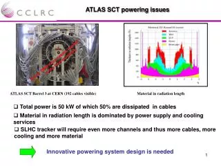
Why independent powering fails at SLHC ?Chip voltage goes down, current stays the same; more channels • Don’t get 5 or 10 times more cables in • Power efficiency is too low (50% ATLAS SCT ~15% SLHC) • Cable material budget: 0.2% of R.L. per layer (barrel normal incidence) 1% or 2% SLHC • Packaging constraints • Each reason by itself is • probably sufficient for a • No-No
History Idea is old, but was only seriously considered a couple of years ago First pioneering work was done by Bonn group for pixels T. Stockmanns, P. Fischer, F. Hugging, I. Peric, O. Runolfsson, N. Wermes, “Serial powering of pixel modules”, Nucl. Instr. & Meth. A511 (2003) 174–179; D. B. Ta, T. Stockmanns, F. Hügging, P. Fischer, J. Grosse-Knetter, Ö. Runolfsson, N. Wermes, “Serial Powering: Proof of Principle demonstration of a scheme for the operation of a large pixel detector at the LHC”, Nucl. Instr. Meth. A557 (2006) 445-459 RAL picked it up 2 years ago for strips Marc Weber, Giulio Villani, Mika Lammentausta, Proceedings of the 11th workshop on electronics for LHC and future experiments, CERN-LHCC-2005-038, (2005) pp. 214-217; Marc Weber, Giulio Villani, “Serial Powering of Silicon Strip Detectors at SLHC”, Proceedings of the 6th “Hiroshima” conference on Silicon detectors (2006); Carl Haber, “A Study of Large Area Integrated Silicon Tracking Elements for the LHC Luminosity Upgrade”, Proceedings of the 6th “Hiroshima” conference on Silicon detectors (2006). Initially main concern was noise; focus moving to system aspects now; reliability; ASIC specs and design
Half-stave setup half-stave AC-Coupling Board Six serially powered ATLAS pixel modules Serial Powering R&D for pixels
Noise studies Module 4 max: 195e- • noise comparison • SP stave versus PP single module operation • effect of one noisy module on the chain • force one module noisy by setting all thresholds to zero • frequency dependent noise pickup negligible Module 1 Module 2 Module 3 max: 400e- Module 3 20kHz Module 4 3MHz Module 5 Module 6 Serial Powering R&D for pixels
Serial powering of six ATLAS SCT modules SP interface board RAL clean room. This was also used for QA of ~800 SCT modules
Noise performance of 6 SCT modules For more details see my talk at the “Hiroshima” conference STD6 • Conclusion is valid for all channels • Gain does not change either • Created noise sources by various means: current injection at different frequencies; HV off for 1 module; increased threshold for 1 module • SP circuitry copes nicely with it Figure 3. Average noise (ENC) for six SCT modules powered independently (IP) or in series (SP). The modules were run for more than 24h before collecting the data shown. The statistical precision of the data points varies between 1.3 and 5 e. Precise measurements; noise performance of SP is excellent
Implement SP on densely packed supermodule For more details see Carl Haber’s talk at the “Hiroshima” conference STD6 Testbed for electrical system design; allows search for noise sources and study G+S issues in challenging packaging arrangement LBNL SP supermodule with 6 hybrids (no sensors) same LBNL SP supermodule with 5 hybrids and 1 module • supermodule is electrically functional and noise performance is promising • This is part of our work program for the next few months
Why is there no conductive interference (noise) between modules? • What about current fluctuations? a) modules cannot sink current, current is conserved no problem (shunt regulators can cope with current fluctuations under normal conditions) • What about voltage fluctuations? a) IR drops are minimum (since current is constant) no damage to regulators, minimum pick-up from power lines b) Module voltage fluctuations do not influence neighbouring modules since voltages are derived by local shunt regulators SP systems tend to be intrinsically quiet; issue of different grounds in a dense environment is being studied by stave program
Off-chip On-chip Off-chip On-chip R R 1.25 1.25 + Offset C C + + - - 1.25 1.25 AC – coupling of signals There are three ways to implement this (slide courtesy Francis Anghinolfi) • Use AC coupling with RC time constant longer than the longer possible “one” state for ABCD protocol 3.6us not preferred solution • Add hysteresis (feed-back) to the chip LVDS receiver works fine for pixel and strips; works in multi-drop bus configuration as well • adopt a RZ or a Manchester encoding on L1 signal Getting AC coupling to run took some effort, but it works
AC LVDS coupling Tested AC LVDS coupling with dedicated test circuits for large range of duty cycles and frequencies 120 MHz 40 MHz 1 MHz This works just fine, not only for DC balanced protocol works for multi-drop bus cables on staves as well We are currently studying this in more detail 1 MHz
Distribution Board 1 • Distribution Board 2 Module 1 Module 2 Module n Power supply Distribution board 1 Distribution board 2 Module n Module 1 Module 2 Digital PS 1 Analog PS 1 Digital PS 2 Analog PS 2 Digital PS n Analog PS n c c b b a a a a Risk due to broken connections: IP vs SP IP SP SP:one broken connection loses n modules, however much less cables (factor 2n less) and less connections
Risk := (# of power connections) x (probability of a failure) x (# of modules lost per failure) Risk ratio (SP/IP) Make your own choices for values of a, b, and c! Mine are here (aSP =1/2 aIP ; b = c = 0) Risk ratio ~ number of modules/4 SP is more risky than IP, but not by much. Risk is manageable if connections are made robust (exploiting the huge real estate gains of SP
Overcurrent protection Power transistor is weak point of SR in case of module failure PT carries full current in case of module open risk of burn out if not cooled properly Protect against this by automatically reducing SR voltage in case of overcurrent condition same idea can be used to set module into “stand-by” mode Simplified diagram for illustration of overcurrent protection Demonstrator board with discrete components performs as simulated voltage reduction from 4V to 1 V while standing full current (~1.5 A)
Overcurrent protection measurements Basic test of the idea using discrete component circuits “Stand-by mode” if over-current voltage decreases from 4V to 1V within 3 ms due to current increase from 40 mA to 1.5 A
Power efficiency Consider n modules with module current and voltages I and V, off-detector cable resistance R, DC-DC gain g, define x= IR/V • power consumed by n modules is always: n I V • power wasted in the cable depends on powering scheme • Low V is bad, large R and I are bad considers cable losses only for now SP: want to have many modules in series DC-DC: want to have few modules in parallel
Regulator power Power [mW] We performed a detailed breakdown of our power consumption of SP circuitry (these were made with a 4 ABCD chip hybrid) • power consumed in PT is ~ (PS current – module current) • power consumed elsewhere is essentially constant Current [mA]
Regulator inefficiency Inefficiency Same date presented as an inefficiency • Note that operating current depends on digital current fluctuations • PT inefficiency dominates for large fluctuations • we measure 10% SP inefficiency • Inefficiency of linear regulator (for analog power) is similar Operating point Current [mA]
Let’s work out a powering example SP: n=20; IH = IPS = 2.4 A; VPS = nVABC-N = 50 VFeatures: saves factor ~8 in power cables/length over SCT hereVABC-N = 2.5 V; IH = 2.4 A; 20 hybrids; DC-DC gain = 20 1 2 3 4 5 6 n-1 n DC-DC PP: n=20; g = 20; IPS = n/g IH = 2.4 A; VPS = gVABC-N = 50 V Features: saves factor ~8 in power cables as SP, watch IR drops RLMT ~ 0.1-1 Ω DC-DC IP: n=1; g = 20; IPS = IH/g = 0.12 A; VPS = gVABC-N = 50 V Features: 2x more cables than SCT problematic for strips
Power efficiency Illustration of various cases: SCT 4V, 1.5 A, R= 4.5 x=1.14; IP ε = 47% SLHC 2.5V, 2.4 A, R= 4.5 x=4.3; SP (only cable losses) SLHC 1.5V, 4 A, R= 4.5 x=12; SP (only cable losses) same but including SR power and LR power (extrapolated from our SCT measurements) Keep hybrid current low! SR inefficiency ~7% for 10% digital current variation LR for analog has similar losses SR inefficiency is reduced for 0.13 m CMOS
Real estate of SP circuitry • Hybrid • SSPPCB Current implementation: 38 x 9 mm2 (this is a PCB for cost reasons) Built 6-module stave with this set-up which is working fine; no redundancy, protection or slow control features • ABCD3TV2 Future implementation: 2-3 ASICs, integrated resistors Redundancy, protection and slow control features Estimated real estate: <12x10 mm2
System design: slow control For IP, we have get information on module voltage and current consumption at external power supply This is not true for SP or PP DC-DC systems It is desirable to implement a slow control system on SLHC silicon tracker modules get rid of sense wires; need to control redundancy and protection features of the new powering circuitry remotely Slow control for new power systems is not part of this talk, but needs attention. Same goes (at later stage) for design of power supplies
Architecture: single or parallel shunt regulator external SR + PT integrated SR + PT RDIC SR and PT Integrated (custom) SR used for Bonn pixel results External commercial SR, used for RAL silicon strip studies Both options work and choice is not obvious
Shunt Regulators I3 I VThres Current [mA] Voltage [V] Number Number Resistance [W] Threshold voltage [V] • Important properties: • Uniformity of threshold voltage • Uniformity of resistance • 3 different shunt regulators on chip: • Nominal 2.0V, 2.4V and 2.7V 285 chips Similar properties verified for the linear regulators
Proposal for design of multi-purpose SP chip SMARP1 block diagram Estimated die size: ~3x3 mm2 Linear regulator (optional) DCS including ADCs • Avoids matching problems between many parallel regulators • Simplifies system and separates functions • Allows for cheap MPW run for SMARP reduce risk and accelerate powering R&D Power transistor (could be separate die) LVDS buffers Shunt regulator We worked out detailed specs for SMARP1, excluding the slow control block The linear regulator is optional and is integrated in the ATLAS ABC-Next The power transistor could be a separate die removing the high-power constraints This is a general-purpose chip, which could be used for ATLAS and CMS; strips or pixels
Vcs+ SOUT Sh sense P1 IN GMT U1 P2 FBS - VREF + PD GND U2 OPM - OPO OPP + /SEN P3 LOUT LIN LSense U3 LM - - FBL + + SMARP regulator elements Shunt regulator and power transistor Over- current protection Linear regulator for analog voltage • Specs are based on experience with commercial devices • Design contains protection and slow control features plus LVDS buffer section for AC coupling (not shown here) • The power transistor P2 could also be an external device (to decouple high and low power objects) • Linear regulator is optional • Additional redundancy is gained by placing 2 SMARPs in parallel
Sketch of a schematic using SMARP - A D H Isrc - -
Features of IP and alternative schemes Let’s preserve the good features of IP have voltage control, current monitoring, and protection features our specs do just that
Outlook • SSPPCB SP offers huge gains in power efficiency, cable and material budget It unusual to gain such significant factors in a technology as mature as silicon detectors Various SP systems have been running since several years now; understanding of system properties is well advanced Noise performance is excellent and we understand why; studies on staves are promising and most generic system tests will be completed this year Next crucial step is to design a custom general-purpose ASIC (SMARP1); this should be a common ATLAS-CMS chip; it would be of interest for pixels and strips; it’s prudent to start this effort soon
Overcurrent protection measurements Basic test of the idea using discrete component circuits Recovery to nominal if current back to normal voltage increase from 1V to 4V within 70 ms due to current decrease from 1.5 A to 40 mA