Advanced Surface Chemistry of Metal and Dielectric Films for Enhanced Material Properties
120 likes | 257 Views
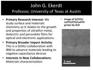
Our research focuses on the materials and surface chemistry of metal films, dielectric coatings, silicon nanostructures, and the catalytic processes involved in biomass conversion. Key objectives include understanding the nucleation and growth processes of these materials, exploring their properties in relation to structure, and developing efficient pathways for lignin depolymerization. Through collaborations and funding from recognized institutions, we aim to innovate in passivation techniques for germanium, investigate high-k dielectric stabilization, and enhance the nucleation of ultrathin metal films.

Advanced Surface Chemistry of Metal and Dielectric Films for Enhanced Material Properties
E N D
Presentation Transcript
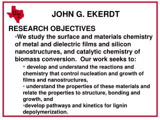
JOHN G. EKERDT RESEARCH OBJECTIVES • We study the surface and materials chemistry of metal and dielectric films and silicon nanostructures, and catalytic chemistry of biomass conversion. Our work seeks to: • develop and understand the reactions and chemistry that control nucleation and growth of films and nanostructures, • understand the properties of these materials and relate the properties to structure, bonding and growth, and • develop pathways and kinetics for lignin depolymerization.
Current Group/Collaborators Funding: AEC, NSF, ONR, SRC, Sirica Corp, Welch
Gate Source Drain Oxide P+ P+ Ge(100) Passivation Layer HfO2 BCN Ge(100) V ISS HfO2 BCN He+ He+ He+ Si(p) Ge CVD Boron Carbo-Nitride as a Germanium Passivation Layer Primary Goal: Explore passivation of Ge with CVD BCxNy films by investigating i) film continuity, ii) oxidation resistance, and iii) electrical properties Motivation Oxidation Resistance During ALD HfO2 deposition Ge has higher charge carrier mobility than Si, but GeO2 is both chemically and electrically unstable. • Passivation layer needed that: • Forms continuous layer on Ge • Resists Ge oxidation • Preserves electrical integrity of Ge ~ 4 nm BCN resists Ge(100) oxidation ISS to determine BCN film continuity BCN Electrical Performance Metal-oxide-semiconductor capacitors (MOSCAPs) fabricated to test electrical properties BCN stoichiometry and growth rate have significant effect on MOSCAP C-V characteristics BCN becomes continuous around 2.5–5 nm on Ge (100)
900℃ 30 sec annealing in N2 SiO2 SiO2 (Pure HfO2) [3Hf+1La]X41 Amorphous [4Hf+1La]X32 Crystallized (~50:50 HfO2:La2O3) Si (100) Si (100) High resolution cross-sectional TEM images ALD growth of high-k dielectric thin films Primary Goal:study the structure and energetics of amorphous films to find ways to stabilize amorphous phases at high temperature MOSFET Metal precursor dosing Motivation: As MOSFET devices scale down, high-k materials are needed for the gate; HfO2 most promising. But HfO2 is easily crystallized Incorporate La Ar purging H2O dosing Ar purging repeat ALD gas delivery system XRD results blue-amorphous, red-crystallized Model of nanolaminate structure
BCxNy Ru(P) ~5 nm SiO2 Si3N4 0.13 μm Ultrathin Amorphous Metal Films Primary Goal: Develop a method for ultrathin (<3nm), continuous films that act as a directly-plateable adhesion promoter and diffusion barrier for Cu IC metallization Barrier ability Amorphous Ru(P) CVD Ru(P) alloy performs comparably to TaN, potential barrier layer ≥165°C Improvement upon diffusion barrier capabilities of pure polycrystalline Ru Improvement upon diffusion barrier capabilities of pure polycrystalline Ru
No CH3I Dielectric Cu Cu 200 nm Liner CH3I Nucleation of Ultrathin Metal Films Primary Goal: Develop fundamental chemical insight needed to improve nucleation and properties of ultrathin metal films that can serve as the barrier/seed liner material. Open via due to Cu diffusion Cu diffusion Liner films will need to be so thin (< 3 nm) that nucleation becomes a significant issue Images courtesy of Sematech Poor nucleation: • Poor nucleation • Large, sparse nuclei • Porous films • Large grains • Rougher films • Good nucleation • Small, dense nuclei • Continuous films • Small grains • Smoother films Good nucleation: 19 nm films No CH3I CH3I 8.5 1010 islands/cm2 18.3 1010 islands/cm2
Directing the CVD Growth of Si Quantum Dots Primary Goal: Develop fundamental chemical insight to permit the precise positioning of quantum dots, and describe how nanostructures assemble on amorphous surfaces. Motivation Controlling the hydride species on Si nanocrystal surface Photoluminescence from passivated Si nanocrystals