Download
1 / 5
50 likes | 73 Views
PCB manufacturing and assembly California understands the need to match with this scenario in each business task and personal glorification. Earlier u2018wire wrapu2019 and u2018point to point constructionu2019 were used, but these options are quite costly from PCB and quite irrelevant in today's digital age. PCB just requires additional design work and other formalities can be automated. It saves the tremendous time of any professional, institutions and students. Visit our online website to know more. https://digitalcoastassembly.com/

E N D
Technology seems an advanced stage of our old tools and measures but this realm is under continuous progress. PCB manufacturing and assembly California understands the need to match with this scenario in each business task and personal glorification. Earlier ‘wire wrap’ and ‘point to point construction’ were used, but these options are quite costly from PCB and quite irrelevant in today's digital age. PCB just requires additional design work and other formalities can be automated. It saves the tremendous time of any professional, institutions and students.
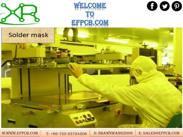
This technological advantage allows components to be correctly connected to a power source with the utmost safety. In addition to it, PCB provides a way to integrate the electronics with your available device in a perfect manner. The continuous evolvement has urged PCB manufacturing and assembly California to provide embellishment to their clients’ business. Maximum boards are manufactured in layers pattern. The base material is used in the middle layer. The usage of copper in its first layer enacts conductive tracks from other sheets and makes the presentation awesome.
CONTACT US CONTACT US Website : - https://digitalcoastassembly.com/ Email Id :- Sales@DigitalCoastAssembly.com Phone No : - 510-495-0450 Address : - 2992 Teagarden St, San Leandro Ca 94577, United States
THANK YOU THANK YOU