Download
1 / 3
30 likes | 124 Views
For pcb design there is testing and validation,functionality and maintenance. Know the stages and smooth process of pcb manufacturing

E N D
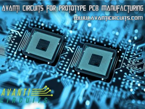
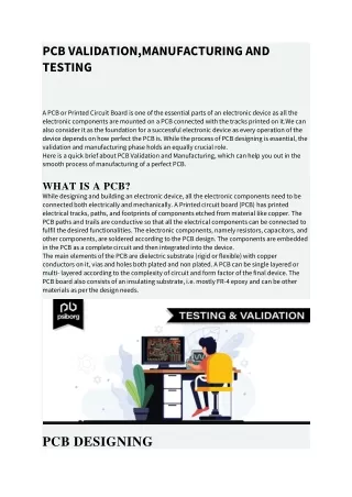
PCB VALIDATION,MANUFACTURING AND TESTING A PCB or Printed Circuit Board is one of the essential parts of an electronic device as all the electronic components are mounted on a PCB connected with the tracks printed on it.We can also consider it as the foundation for a successful electronic device as every operation of the device depends on how perfect the PCB is. While the process of PCB designing is essential, the validation and manufacturing phase holds an equally crucial role. Here is a quick brief about PCB Validation and Manufacturing, which can help you out in the smooth process of manufacturing of a perfect PCB. WHAT IS A PCB? While designing and building an electronic device, all the electronic components need to be connected both electrically and mechanically. A Printed circuit board (PCB) has printed electrical tracks, paths, and footprints of components etched from material like copper. The PCB paths and trails are conductive so that all the electrical components can be connected to fulfil the desired functionalities. The electronic components, namely resistors, capacitors, and other components, are soldered according to the PCB design. The components are embedded in the PCB as a complete circuit and then integrated into the device. The main elements of the PCB are dielectric substrate (rigid or flexible) with copper conductors on it, vias and holes both plated and non plated. A PCB can be single layered or multi- layered according to the complexity of circuit and form factor of the final device. The PCB board also consists of an insulating substrate, i.e. mostly FR-4 epoxy and can be other materials as per the design needs. PCB DESIGNING
PCB designing is the process of designing the circuitry using potential PCB Design Softwares such as Altium, Eagle, Ki-Cad, Easyeda etc, consisting of a diverse essential PCB tools helping us to make a perfect Design, and also runs a DFM (Design for Manufacturability) check so that no problem is faced during manufacturing.A perfect PCB is designed, keeping in mind the complete requirements of the device. The design is tested as per the requirements with the help of simulations. Let’s understand the process in detail. TESTING AND VALIDATION: TESTING THE PROTOTYPE AND VALIDATING IT WITH THE SOFTWARE After the PCB design is complete, the next step is to manufacture a prototype and to test it with various conditions and constraints to assure the quality and robustness of the hardware. The prototype and it’s application or dashboard needs to be validated before taking it forward for manufacturing processes. The different parameters of the hardware such as signals, voltages, amplitude, magnitude, temperatures, heat conditions, the power consumption etc. are tested. The prototype is created several times till the final prototype is ready covering all the requirements of the client. The final prototype is the one that fits with the client requirements thoroughly, and the client approves it for manufacturing. At the end of this stage, the delivery of the prototypes, design files, test reports, estimates, and a detailed set of future recommendations is done. MANUFACTURING: FABRICATION OF THE PRINTED CIRCUIT BOARD AND IT’S ASSEMBLY The manufacturing of the product can be done for bulk products. The test such as stress testing, defects identification, individual components testing is performed for the product after the first batch manufacturing, for quality check and to reduce rejection.After the issues are identified, the reason for the problem is checked, and the rectification of the problem is started. MAINTENANCE: PRODUCT LIFETIME SUPPORT. After all the stages, as mentioned above, get completed, the product is marked complete. Now the maintenance part starts. The product needs modifications from time to time to remain up to date with the technologies. The engineers and programmers provide maintenance throughout the product lifetime. The firmware updates are provided, and new features are updated every now and then.
This is the last stage of IoT Product lifecycle. The process of PCB validation and manufacturing is not only vast but also fundamental while making an electronic device. The process is crucial as the slightest mistake can lead to failure of the product. PSIBORG TECHNOLOGIES PCB DESIGN SERVICES Are you looking for a professional PCB design services provider? If yes, then you need to make sure that the service provider you are choosing performs every step with transparency and professionalism. We at PsiBorg Technologies make sure that we provide the best PCB design services for a perfect IoT Product.