Magic triangle
Magic triangle. Materials science epitaxy, self organized growth organic synthesis implantation, isotope purification atom and molecule manipulation nanolithography, nanoprinting beam and scanning probes. Magic triangle. Physics of complex systems

Magic triangle
E N D
Presentation Transcript
Magic triangle Materials science epitaxy, self organized growth organic synthesis implantation, isotope purification atom and molecule manipulation nanolithography, nanoprinting beam and scanning probes ....
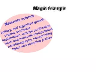
Magic triangle Physics of complex systems exotic ground states and quasiparticles phase and statistical transformations complex dynamics …. Materials science epitaxy, self organized growth organic synthesis implantation, isotope purification atom and molecule manipulation nanolithography, nanoprinting beam and scanning probes ....
Magic triangle Physics of complex systems exotic ground states and quasiparticles phase and statistical transformations complex dynamics …. Materials science epitaxy, self organized growth organic synthesis implantation, isotope purification atom and molecule manipulation nanolithography, nanoprinting beam and scanning probes .... High tech/IT photonics (optoelectronics) MEMS, NEMS electronics, magnetoelectronics spintronics ….
SEMICONDUCTOR SPINTRONICS Tomasz DIETL Institute of Physics, Polish Academy of Sciences, Warsaw • Why spin electronics? -- semiconductors -- ferromagnetic metals 2. Ferromagnetic semiconductors 3. Spin manipulation -- magnetization -- single spins reviews: listed in the abstract
Integrated circuits 2002 4 transistors109transistors processing and dynamic storage of information ; P i DRAM J. S. Kilby US Patent Office, 3 052 822
Field effect transistorSi-MOS-FET gate source drain MOSFET – resistor + capacitor Two states: conducting/non-conducting eg. multiplication (AND)
„semiconductor” Cu2S drain, Al source, Al gate Al foil glass substrate US Patent Office, 1 745 175 MES FET
Julius Edgar Lilienfeld (1882-1963) Born in 1882 and till 1899 in Lvov Study and PhD(1905)in Berlin Professorin Leipzig (1910-26) Since 1926 in USA Kleint, Prog. Surf. Sci. ‘98
Storing of information on hard disk • high density and non-volatile (5GB/cm2 ) • slow access and non-reliable (moving parts)
Storing of information on magnetooptical disc H < Hc T > TC • writing: heating above TC • reading: Kerr effect
Barriers • financial, legal, psychological, ... • technical - heat release, defects in oxide, .... • physical - grain structure of matter: Coulomb blockade, ... - quantum phenomena: interference, tunneling, ... - thermodynamic phenomena: superparamagnetism, ... • entertainment industry • … Driving forces nanotechnology
New information carrier - electron photon, flux (SQUID loops), vortex (type II superconductors); - spin rather than charge ... • New principle of device operation quantum devices, spin transistors, ... • New architecture - physical, chemical and biological processes - quantum computing • Integration of functions, not only elements => Spintronics
SPINTRONICS exploiting spin, not only charge rational: spin robust to external perturbations • Storing and processing of classical information • Storing and processing of quantum information • Sensing magnetic field
Giant magnetoresistance (GMR) in ferromagnetic metal multilayers 4.2 K A. Fert et al., P. Gruenberg et al., S. Parkin et al., 1988-91 J. Barnaś et al. (theory)
Information reading GMR/TMR sensors IBM 1997- GMR TMR
Magnetic random access memory (MRAM) Infineon, Motorola, 256 kb • non-volatile • fast (50 ns) • reliable • radiation hardness • .... • Difficulties: • thin oxide, 1.2 nm • large writing currents • ...
Spintronics – material aspects Why to do not combine complementary properties and functionalities of semiconductor and magnetic material systems? • hybrid structures -- overlayers or inclusions of ferromagneticmetals =>source of stray fields and spin-polarized carriers -- soft ferromagnets => local field amplifiers -- hard ferromagnets => local field generators (cf. J. Kossut, ILC, Budapest’02) • ferromagnetic semiconductors
Ferromagnetic semiconductors • magnetic semiconductors short-range ferromagnetic super- or double exchange EuS, ZnCr2Se4, La1-xSrxMnO3, ... • diluted magneticsemiconductors long-range hole-mediated ferromagnetic exchange IV-VI: p-Pb1-x-yMnxSnyTe(Story et al.’86) III-V: In1-x-MnxAs (Munekata et al.’89,’92) Ga1-x-MnxAs(Ohno et al.’96) TC 100 K for x = 0.05 II-VI: Cd1-xMnxTe/Cd1-x-yZnxMgyTe:N QW (Cibert et al.’97, Kossacki et al.’99) Zn1-xMnxTe:N (Ferrand et al.’99)Be1-xMnxTe:N (Hansen et al.’01) III-V and II-VI DMS: quantum nanostructures and ferromagnetism combine
Spin injection in p-i-n(Ga,Mn)As /(In,Ga)As/GaAs diode (spin-LED) Polarization (%) Ohno et al., Nature ‘99
The nature of the Mn state and its coupling to carriers Mn: 3d54s2 II-VI: Mn electrically neutral (3d5, S = 5/2) –doping by acceptors necessary III-V: Mn acts as source of spins and holes • large p-d hybridization and large intra-site Hubbard U => Kondo hamiltonian H = -NoSs => large Mn-hole exchange -- (Ga,Mn)As: No- 1.2 eV(Szczytko et al., Okabayashi et al.) -- (Zn,Mn)Te: No- 1.0 eV(Twardowski et al.) • no s-d hybridization => small Mn-electron exchange No0.2 eV (Gaj et al.)
k Mean-field Zener model Which form of Mn magnetizationminimizes F[M(r)]? F = FMn[M(r)] + Fholes[M(r)] M(r) 0for H= 0 at T < TC ifM(r)uniform => ferromagnetic order otherwise => modulated magnetic structure nholes <<Nspins Zener RKKY
Curie temperature in p-Ga1-xMnxAstheory vs.experiment • Anomalous Hall effect p uncertain • Omiya et al.: 27 T, 50 mK • Theory: TC > 300 K for x > 0.1 and large p T.D. et al., PRB’01
Tuning of magnetic ordering by electrostatic gates (ferro-FET) H. Ohno, .., T.D., ...Nature ‘00
Ferromagnetic temperature in 2D p-Cd1-xMnxTe QW and 3D Zn1-xMnxTe:N (k) 1018 1019 1020 cm-3 3D k (k) 2D k (k) 1D H. Boukari, ..., T.D., PRL’02 D. Ferrand, ... T.D., ... PRB’01 k
Control by electrostatic gate in a pin diode – ferro-LED V p doped QW undoped barriers n doped Photoluminescence Ec EF V Ev Hole liquid Depleted PRL’02
Combined: electrostatic gate + illumination in pin diode (ferro-LED) V 1.5 K 0 V Ec EF Ev QW illumination Hole liquid Depleted Ferro- diode: electric field and light tuned ferromagnetism V PRL ‘02
Optical tuning of magnetization - pip diode paramagnetic Ec Hole concentration Temperature Illumination EF Ev CdMnTe QW 8 nm 0 to 4% Mn T = const p = const ferromagnetic PRL’02 pip diode: light destroys ferromagnetism
Zinc-blende ferromagnetic semiconductors- highlights • Spin injection - (Ga, Mn)As/(Ga,In)As(St. Barbara, Sendai) • Dimensional effects (Cd,Mn)Te, (Zn,Mn)Te (Grenoble, Warsaw) • Isothermal transition para <--> ferro - light (In,Mn)As (Tokyo); (Cd,Mn)Te (Grenoble, Warsaw) - electric field (In,Mn)As (Sendai); (Cd,Mn)Te (Grenoble, Warsaw) • GMR (Ga, Mn)As/(Al,Ga)As/ (Ga, Mn)As (Sendai) • TMR (Ga, Mn)As/AlAs/ (Ga, Mn)As (Sendai, Tokyo) • MCD(Ga, Mn)As (Warsaw, Tsukuba, St. Barbara) • Strain engineering (Ga, Mn)As (Sedai, Tokyo, Warsaw)
Chemical trends – hole driven ferromagnetism xMn = 0.05, p = 3.5x1020 cm-3 Materials of light elements: • large p-d hybridization • small spin-orbit interaction T.D. et al., Science ‘00
Quantum information hardware A model of quantum computer, 28Si:31P • qubit: nuclear spin I = ½ of Phosphorous donor impurity • single qubit operations: A gates affect hyperfine interaction • two qubit operations: J gates affect e-e exchange interaction • silicon: 28Si – no nuclear moments, weak spin-orbit interaction Kane, Nature’98 cf. Loss, DiVincenzo PRA’98
Towards quantum gates of quantum dots expl. Delft, Munich, Ottawa, Rehovot, Tokyo, Warsaw, Wuerzburg, …. theory: Basel, Modena, Ottawa, Paris, Sapporo, Wroclaw, … Spin molecules: cf. B. Barbara talk Quantum optics: cf. A. Zeilinger talk
Summary: trends in semiconductor spintronics • Physics of spin currents -- injection, transport, coherence, new devices • Spin manipulation -- isothermal and fast magnetization reversal -- single spin manipulation, magnetometry, entanglement • Search for high temperature ferromagnetic semiconductors -- carrier-controlled ferromagnetism -- intrinsic ferromagnetism warning: precipitates and inclusions often present Thanks to colleagues in Warsaw and to: I. Solomon, Y. Merle d’Aubigne, H. Ohno, A.H. MacDonald, …