MPU Communication and Bus Timing
Understand the instruction cycle of microprocessors - fetch and execute cycles, machine cycles, T-states, and operations. Learn about MPU communication and bus timing with detailed examples and diagrams.

MPU Communication and Bus Timing
E N D
Presentation Transcript
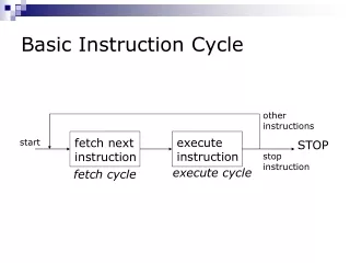
Instruction cycle • Instruction: A command given to the microprocessor to perform an operation • Program : A set of instructions given in a sequential manner to perform a particular task The CPU fetches one instruction from memory at a time & executes it. Instruction cycle = Fetch cycle + Execute cycle
Fetch Cycle : The steps taken by CPU to fetch the opcode from the memory The time taken for fetch cycle is fixed. Execute Cycle : The steps taken by CPU to fetch data & to perform the operation specified in the instruction The time taken for execute cycle is variable which depends on the type of instruction ,i.e. 3 –byte , 2-byte & 1-byte instruction.
Machine cycle The time required by the micro processor to complete the operation of accessing memory or I/O device . Operations like : • Opcode fetch • Memory read • Memory write • I/O read • I/O write
T - states Microprocessor performs an operation in specific clock cycles. Each clock cycle is called as T –States. The number of T – states required to perform an operation is called Machine Cycle .
MPU Communication and Bus Timing Figure 3: Moving data form memory to MPU using instruction MOV C, A (code machine 4FH = 0100 1111)
MPU Communication and Bus Timing The Fetch Execute Sequence : 1. The μp placed a 16 bit memory address from PC (program counter) to address bus. Figure 4: at T1 • The high order address, 20H, is placed at A15 – A8. • the low order address, 05H, is placed at AD7 - AD0 and ALE is active high. • Synchronously the IO/M is in active low condition to show it is a memory operation. 2. At T2 the active low control signal, RD, is activated so as to activate read operation; it is to indicate that the MPU is in fetch mode operation.
MPU Communication and Bus Timing 3. T3: The active low RD signal enabled the byte instruction, 4FH, to be placed on AD7 – AD0 and transferred to the MPU. While RD high, the data bus will be in high impedance mode. 4. T4: The machine code, 4FH, will then be decoded in instruction decoder. The content of accumulator (A) will then copied into C register at time state, T4.
S0 and S1Pin 29 (Output) and Pin 33 (Output) • S0 and S1 are called Status Pins. • They tell the current operation which is in progress in 8085. Haramardeep Singh
Table Showing IO/M, S0, S1 and Corresponding Operations Haramardeep Singh
MPU Communication and Bus Timing Figure 4: 8085 timing diagram for Opcode fetch cycle for MOV C, A .
Memory Read: The flow of data from the memory to the microprocessor. Step 1(T1) : microprocessor places the address on the address lines from program counter & activates ALE signal to multiplex the low order address. It also sends status signals IO/M = 0, S1=1, S0 =0 for memory read operation. Step 2 (T2) : SE