Memory and Programmable Logic
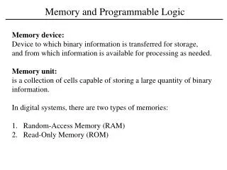
Memory and Programmable Logic. Chapter 7. 7-1 Introduction. Memory information storage a collection of cells store binary information RAM – Random-Access Memory read operation write operation ROM – Read-Only Memory read operation only a programmable logic device.

Memory and Programmable Logic
E N D
Presentation Transcript
Memory and Programmable Logic Chapter 7
7-1 Introduction • Memory • information storage • a collection of cells store binary information • RAM – Random-Access Memory • read operation • write operation • ROM – Read-Only Memory • read operation only • a programmable logic device
Programmable Logic Device (PLD) • ROM • PLA – programmable logic array • PAL – programmable array logic • FPGA – field-programmable gate array • programmable logic blocks • programmable interconnects Fig. 7.1 Conventional and array logic diagrams for OR gates
7-2 Random-Access Memory • A memory unit • stores binary information in groups of bits (words) • 8 bits (a byte), 2 bytes, 4 bytes • Block diagram Fig. 7.2 Block diagrams of a memory unit
A 1024 16 Memory Fig. 7.3 Contents of a 1024 16 memory
Write and Read Operations • Write operation • Apply the binary address to the address lines • Apply the data bits to the data input lines • Activate the write input • Read operation • Apply the binary address to the address lines • Activate the read input
Memory Description in HDL • Examples
Timing Waveforms • The operation of the memory unit is controlled by an external device • The access time • the time required to select a word and read it • The cycle time • the time required to complete a write operation • Read and write operations must synchronized with an external clock
CPU clock – 50 MHz • The access/cycle time < 50 ns • A write cycle Fig. 7.4 Memory cycle timing waveforms
A read cycle Fig. 7.4 Memory cycle timing waveforms (cont.)
Types of Memories • Static • Information are stored in latches • remains valid as long as power is applied • short read/write cycle • Dynamic • Information are stored in the form of charges on capacitors • the stored charge tends to discharge with time • need to be refreshed (read and write back) • reduced power consumption • Larger memory capacity
Volatile • lose stored information when power is turned off • SRAM, DRAM • Non-volatile • Retains its stored information after the removal of power • ROM • EPROM, EEPROM • Flash memory
7-3 Memory Decoding • A memory unit • the storage components • the decoding circuits to select the memory word • A memory cell Fig. 7.5 Memory cell
Internal Construction • A RAM of m words and n bits per word • m*n binary storage cells • Decoding circuits to select individual words • k-to-2k decoder
A 4 4 RAM Fig. 7.6 Diagram of a 4 4 RAM
Coincident Decoding • A two-dimensional selection scheme • reduce the complexity of the decoding circuits Fig. 7.7 Two-dimensional decoding structure for a 1K-word memory
A 10-to-1024 decoder • 1024 AND gates with 10 inputs per gates • Two 5-to-32 decoders • 2 * (32 AND gates with 5 inputs per gates) • Reduce the circuit complexity and the cycle time
Address Multiplexing • The reduce the number of pins in the IC package • consider a 64M1 DRAM • 26-bit address lines • Multiplex the address lines in one set of address input pins
An examples • RAS – row address strobe • CAS – column address strobe Fig. 7.8 Address multiplexing for a 64K DRAM
Random Access Memory 第三版內容,參考用! RAS, CAS Addressing Even to read 1 bit, an entire 64-bit row is read! Separate addressing into two cycles: Row Address, Column Address Saves on package pins, speeds RAM access for sequential bits! Read Cycle Read Row Row Address Latched Read Bit Within Row Column Address Latched Tri-state Outputs
Random Access Memory 第三版內容,參考用! Write Cycle Timing (1) Latch Row Address Read Row (2) WE low (3) CAS low: replace data bit (4) RAS high: write back the modified row (5) CAS high to complete the memory cycle
7-4 Error Detection And Correction • Improve the reliability of a memory unit • A simple error detection scheme • a parity bit (Sec. 3-9) • a single bit error can be detected, but cannot be corrected • An error-correction code • generates multiple parity check bits • the check bits generate a unique pattern, called a syndrome • the specific bit in error can be identified
Hamming Code • k parity bits are added to an n-bit data word • (2k –1 n + k) • The bit positions are numbered in sequence from 1 to n + k • Those positions numbered as a power of 2 are reserved for the parity bits • The remaining bits are the data bits
Example: 8-bit data word 11000100 • Include 4 parity bits and the 8-bit word 12 bits 2k –1 n + k, n = 8 k = 4 Bit position: 1 2 3 4 5 6 7 8 9 10 11 12 P1P2 1 P4 1 0 0 P8 0 1 0 0 • Calculate the parity bits: even parity assumption P1 = XOR of bits (3, 5, 7, 9, 11) = 1 1 0 0 0 = 0 P2 = XOR of bits (3, 6, 7, 10, 11) = 1 0 0 1 0 = 0 P4 = XOR of bits (5, 6, 7, 12) = 1 0 0 0 = 1 P8 = XOR of bits (9, 10, 11, 12) = 0 1 0 0 = 1 • Store the 12-bit composite word in memory. Bit position: 1 2 3 4 5 6 7 8 9 10 11 12 00 1 1 1 0 0 1 0 1 0 0
When the 12 bits are read from the memory • Check bits are calculated C1 = XOR of bits (1, 3, 5, 7, 9, 11) C2 = XOR of bits (2, 3, 6, 7, 10, 11) C4 = XOR of bits (4, 5, 6, 7, 12) C8 = XOR of bits (8, 9, 10, 11, 12) • If no error has occurred Bit position: 1 2 3 4 5 6 7 8 9 10 11 12 0 0 1 1 1 0 0 1 0 1 0 0 C = C8C4C2C1 = 0000
One-bit error • error in bit 1 • C1 = XOR of bits (1, 3, 5, 7, 9, 11) = 1 • C2 = XOR of bits (2, 3, 6, 7, 10, 11) = 0 • C4 = XOR of bits (4, 5, 6, 7, 12) = 0 • C8 = XOR of bits (8, 9, 10, 11, 12) = 0 • C8C4C2C1 = 0001 • error in bit 5 • C8C4C2C1 = 0101 • Two-bit error • errors in bits 1 and 5 • C8C4C2C1 = 0100
The Hamming code can be used for data of nay length • k check bits • 2k –1 n + k
Single-Error Correction, Double-Error Detection • Hamming code • Can detect and correct only a single error • Multiple errors may not be detected. • Hamming code + a parity bit • Can detect double errors and correct a single error. • The additional parity bit is the XOR of all the other bits. • E.g.: the previous 12-bit coded word 0 0 1 1 1 0 0 1 0 1 0 0 P13 0 0 1 1 1 0 0 1 0 1 0 0 1 (even parity).
When the word is read from memory • If P = 0, the parity is correct; P = 1, incorrect • Four cases • If C = 0, P = 0, no error • If C 0, P = 1, a single error that can be corrected • If C 0, P = 0, a double error that is detected but cannot be corrected • If C = 0, P = 1, an error occurred in the P13 bit
7-5 Read-Only Memory • Store permanent binary information • 2k x n ROM • k address input lines • enable input(s) • three-state outputs Fig. 7.9 ROM block diagram
32 x 8 ROM • 5-to-32 decoder • 8 OR gates • each has 32 inputs • 32x8 internal programmable connections Fig. 7.10 Internal logic of a 32 8 ROM
programmable interconnections • close (two lines are connected) • or open • A fuse that can be blown by applying a high voltage pulse Fig. 7.11 Programming the ROM according to Table 7.3
ROM truth table (partial) • an example
Combinational Circuit Implementation • ROM: a decoder + OR gates • sum of minterms • a Boolean function = sum of minterms • For an n-input, m-output combinational ckt 2n m ROM • Design procedure: • Determine the size of ROM • Obtain the programming truth table of the ROM • The truth table = the fuse pattern
Example 7-1 • 3 inputs, 6 outputs • B1=0 • B0=A0 • 8x4 ROM
ROM implementation • Truth table Fig. 7.12 ROM implementation of Example 7.1
Types of ROM • Types of ROM • mask programming ROM • IC manufacturers • is economical only if large quantities • PROM: Programmable ROM • fuses • universal programmer • EPROM: erasable PROM • floating gate • ultraviolet light erasable • EEPROM: electrically erasable PROM • longer time is needed to write • flash ROM • limited times of write operations
Combinational PLDs • Programmable two-level logic • an AND array and an OR array Fig. 7.13 Basic configuration of three PLDs
7.6 Programmable Logic Array • PLA • an array of programmable AND gates • can generate any product terms of the inputs • an array of programmable OR gates • can generate the sums of the products • more flexible than ROM • use less circuits than ROM • only the needed product terms are generated
F1 = AB + AC + ABC • F2 = (AC + BC) • XOR gates • can invert the outputs • An example Fig. 7.14 PLA with three inputs, four product terms, and two outputs
PLA programming table • specify the fuse map
The size of a PLA • The number of inputs • The number of product terms (AND gates) • The number of outputs (OR gates) • When implementing with a PLA • reduce the number of distinct product terms • the number of terms in a product is not important
Examples 7-2 • F1(A, B, C) = (0, 1, 2, 4); F2(A, B, C) = (0, 5, 6, 7) • both the true value and the complement of the function should be simplified to check Fig. 7.15 Solution to Example 7.2
F1 = (AB+ AC + BC) • F2 = AB + AC + ABC Fig. 7.14 PLA with three inputs, four product terms, and two outputs
7-7 Programmable Array Logic • a programmable AND array and a fixed OR array • The PAL is easier to program, but is not as flexible as the PLA 第三版圖片,參考用!
An example PAL • product terms cannot be shared Fig. 7.16 PAL with fourinputs, four outputs, and a three-wide AND-OR structure
An example implementation w(A,B,C,D) = (2,12,13) x(A,B,C,D) = (7,8,9,10,11,12,13,14) y(A,B,C,D) = (0,2,3,4,5,6,7,8,10,11,15) z(A,B,C,D) = (1,2,8,12,13) • Simplify the functions w = ABC + ABCD x = A + BCD y = AB + CD + BD z = ABC + ABCD + ACD + ABCD = w + ACD + ABCD
w = ABC + ABCD • x = A + BCD • y = AB + CD + BD • z = w + ACD + ABCD Fig. 7.17 Fuse map for PAL as specified in Table 7.6