Download
1 / 25
250 likes | 428 Views
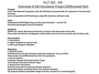
ELCT 361 - EM Overview of EM Simulation Project (Differential Pair). Purpose : Learn how Maxwell’s equations solve the EM fields associated with the operation of an electronic structure. Learn Computational EM techniques using EM simulation software tools. Tools :

E N D
ELCT 361 - EM Overview of EM Simulation Project (Differential Pair) Purpose: Learn how Maxwell’s equations solve the EM fields associated with the operation of an electronic structure. Learn Computational EM techniques using EM simulation software tools. Tools: Ansys/Ansoft HFSS (High Frequency Structure Simulator - version 14). Ansys/Ansoft Designer (Circuit Simulator) Operation: Divides up a three-dimensional electronic structure into thousands of tiny cells. Then solves the Electric and Magnetic Fields within each cell as they interact with all other cells. Files Provided: 1. Instructions. 2. Report template (in ppt format). 3. HFSS and Designer templates. Objectives: 1. Draw Structure. PCB (Printed Circuit Board) Stack-up (Ground, Dielectric, Trace, Air Box). Transmission Line (Differential Pair, Ports for excitation). 2. Set up Analysis. Frequency Domain (Terminal Solution Type) Time Domain (Transient Solution Type) 3. Results from Simulation. Channel Losses (from Frequency Domain Analysis). Signal Attenuation and Delay (from Time Domain Analysis). Eye Diagram (Defines allowable voltage and time variation of a received signal).
HFSS Windows Tool Bar Project Mgr Model Report Boundaries Air Box Graphs Excitations Ground Analysis Optimetrics Traces Markers Results Dielectric Properties Ports Independent Variables Model Tree Dependent Variables Message Progress
1.Structure Overview. Differential Pair T3 Air Box 3-D View T4 Port 2 Differential Pair Differential Pair Dielectric Port 1 T1 T2 Front View- Stack up Copper Traces Copper Traces Port Dielectric Layer Ground
1.Draw Structure. Detail of Ground, Dielectric, Ports z -(wPort/2),LT,hG y wPort=10*wT+xD Port2 Board -(wPort/2),0,hG xD Port1 -(xD/2+Board),0,0 Origin Dielectric LT hPort=8*hD Ground Location of coordinates: Ground Dielectric Ports x
1.Draw Structure. Detail of Differential Pair (The “Trapezoidal” shape is typical of manufactured traces.) Location of coordinates to form “Trapezoidal” shape. -(gT/2+wT-xT),0,(hG+hD+hT) -(gT/2+xT),0,(hG+hD+hT) xT Trace 1 Trace 2 hT Copper gT wT Dielectric -(gT/2+wT),0,(hG+hD) hD FR4 -(gT/2),0,(hG+hD) z Ground hG x Copper Origin
2.Analysis Set-ups (must do). Windows Explorer HFSS Options 2. Then add these 2 files and open 1. Create this folder under “Temp” in the C: drive 3. Set these options under: >Tools >Options >HFSS Options 3. Set these options under: <Tools >Options >HFSS Options
2.Analysis Set-ups (already done). Design Properties (Variables) Solution Setup Frequency Sweep Excitations Differential Pairs
2.Analysis Set-ups (already done). Report Parametric Sweep
3.Results. Frequency Plots. 3.Results. Transient Plots. 1cm 5cm 10cm 1cm 5cm dB mV 10cm 20cm 20cm Attenuation, Delay S21-Insertion Loss Freq (GHz) Time (us) 1cm 5cm 10cm 20cm 1cm V 5cm dB 10cm 20cm Eye Diagram S21-Insertion Loss Freq (GHz) Time (us)
EYE DIAGRAM. Time Domain. Eye Diagram: Superimpose consequetive bits in a data stream Statistical Analysis 1 0 0 1 1 0 1
EYE DIAGRAM. Time Domain. Eye Diagram: Superimpose consequetive bits in a data stream Statistical Analysis Bit 0 0 1 1 0 1 1
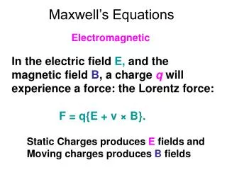
S-Parameters. Frequency Domain. S11 (Return Loss) S21 (Insertion Loss) Po Po Pi 2-Port Network 2-Port Network Port 1 Port 2 Port 1 Port 2 Pi Prefer to have least amount of power reflected (eg: Po/Pi = 1/10) Prefer to have more power pass through to load (eg: Po/Pi = 5/10) S11 S21 example example 0 0 Prefer large negative dB dB dB Prefer near to zero dB -10 -10 37 freq freq
Frequency Plot. 1cm S-Parameters S21 S11 dB Frequency
Designer Circuit Circuit Components HFSS Model Probes Probes
Elct 361. EM Simulation Project Report. Fall 2013. Name: Date: Specification: A. Ansoft HFSS (Structure Simulator). 1. Draw structure in Ansoft HFSS (Transient). 2. Set up Attributes, Excitation , and Boundary Conditions. 3. Simulate the design. 4. Results: a. Time Domain (Transient). b. Frequency Domain (Spectral). B. Ansoft Designer (Circuit Simulator). 1. Set up Signal Generator Circuit in Ansoft Designer. 2. Import HFSS Model. 3. Simulate the Circuit (Vary “Data Rate” to get EYE opening). 4. Results. a. EYE Diagram.
HFSS Operation 1. HFSS Solution Process. (C:\Program Files (x86)\Ansoft\HFSS14.0\Win64\Help\ hfss_onlinehelp Ch 18 p 2-5.) FEM. (eg: HFSS uses FEM (Finite Element Method) to mesh the Computational Domain. FEM divides this space into thousands of smaller elements or cells called tetrahedrals (three-dimensional triangles).) Matrix Equations. Basis Functions. Adaptive Analysis. HFSS Solution Process. 2. Solution of Maxwell’s equations. (C:\Program Files (x86)\Ansoft\HFSS14.0\Win64\Help\ hfss_onlinehelp Ch 18 p 36-39.) “Maxwell’s Equations” Ch 7. p. 205-206. Maxwell’s Equations. DGTD Solver. (eg: each mesh element advances in time using its own time step in a synchronous manner. This results in a significant speed-up.) Parallelism.
HFSS Model 3D View Air Box Trace Dielectric Port Ground Identify figure (eg: This is a figure of a Microstrip line drawn in “HFSS” for analyzing the transient and spectral characteristics.) Describe components. (eg: The Air Box confines the computational domain to within ¼ wavelength from conducting surfaces in order to model the radiation of EM waves in space while also reducing the simulation time.)
Transient Plot Voltage In (5cm) Voltage Out (5cm) Identify plot (eg: This is a plot of a broadband pulse in the time domain over the interval …ps) Compare time delay and attenuation due to the trace length (from delta markers on plot). Compare results for time delay from plot with empirical formulation (from formula below).
Frequency Plot (1) Differential Pair Differential Pair S21 5cm Differential Pair S21 10cm Differential Pair S21 20cm Identify plot (eg: This is a plot of the insertion losses in the frequency domain for a Differential Pair of Traces over the interval …GHz) Compare insertion losses (S21) due to the trace lengths and frequency (from maximum markers on plot). [The interval between resonant troughs for the S11 graph (not shown. Change step size to 0.1GHz and rerun. Takes 5x longer.) can be approximated by the formulation given below.]
Frequency Plot (2) Single-Ended Trace Single-Ended S21 5cm Single-Ended S21 10cm Single-Ended S21 20cm Identify plot (eg: This is a plot of the insertion losses in the frequency domain for a Single-Ended Trace over the interval …GHz) Compare insertion losses (S21) due to the trace lengths and frequency (from maximum markers on plot).
Frequency Plot (3) Compare Diff and S-E Differential Pair S21 5cm Single-Ended S21 5cm Identify plot (eg: This is a plot in the frequency domain comparing the insertion losses for a Differential Pair and a Single-Ended Trace over the interval …GHz) Compare insertion losses (S21) due to the type of transmission line (from maximum markers on plot).
Designer Circuit HFSS Model Pseudo Random Binary Source Binary to M-ary Coder Symbol Repeater Root Raised Cosine Filter Bit Error Rate Probe Signal Probe Identify figure (eg: This is a Signal Generator circuit drawn in “Designer” for analyzing the EYE Diagram and BER (Bit Error Rate)) Describe components. (eg: The PSRB assigns ___ random bits at a rate of ___ GHz .)
Designer EYE Diagram. EYE Mask. 5cm Voltage level Acceptable Time duration of signal Identify plots. (eg: This figure is the EYE Diagram in the time domain for the EYE opening of a 5 cm line at the data rate of ___ over the interval 1/rate = ___.) Analyze plots. (eg: Notice that the Voltage and Time differential fall within the given constraints of the EYE Mask for the 5 cm line.) Define eye diagram. An eye diagram is a graph that measures the voltage and time variations in a signal caused by the signal channel. It is constructed by superimposing numerous consecutive bits in a data stream.
Conclusion HFSS tool: (C:\Program Files\Ansoft\HFSS14.0\Win64\Help\hfss_onlinehelp p1-1) HFSS simulation results: Designer tool : (C:\Program Files\Ansoft\Designer7.0\Windows\Help\getstart p 4-1, 5-1, nexxim p 1-10, 1-12). Designer simulation results: