Overview of Single Cycle Processor Architecture and ALU Control Signals
This document provides a comprehensive overview of the single-cycle processor architecture, focusing on the data path controls, ALU operations, and instruction decoding. It covers fundamental components such as the ALU, control signals, and memory operations crucial for executing R-type and I-type instructions. The control unit's role in signal generation based on instruction opcodes and function codes is detailed, along with practical examples. It encapsulates how data flows through registers, the ALU’s operations like addition and subtraction, and the significance of opcode in controlling the processor's functionalities.

Overview of Single Cycle Processor Architecture and ALU Control Signals
E N D
Presentation Transcript
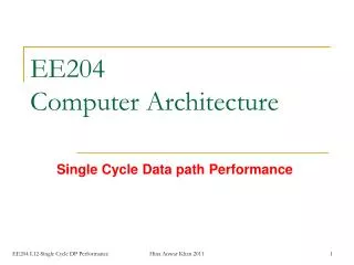
EE204Computer Architecture Processor Data path Control Hina Anwar Khan 2011
Single Cycle Processor Data path 0 4 Result 1 clk Add Result Sh.Left2 Add Single-Cycle Design Read reg. num A Read reg num A Read address Read reg data A Data Memory Read reg num B Read address PC Zero Read data 1 Registers Instruction [31-0] Write address Result Write reg num InstructionMemory 0 0 Read reg data B Write data Write reg data 1 clk clk 16 32 signextend Hina Anwar Khan Spring 2011
Operation BInvert CarryIn A 0 1 Result 0 B + 2 1 3 Less CarryOut The ALU • The ALU is stuck right in the middle of everything... • It must: • Add, Subtract, And, or Or for arithmetic instructions • Subtract for a branch on equal • Subtract and set for a SLT • Add for a memory access Function BInvert Op Carryin Result And 0 00 0 R = A • B Or 0 01 0 R = A Ú B Add 0 10 0 R = A + B Subtract 1 10 1 R = A - B SLT 1 11 1 R = 1 if A < B 0 if A ³ B Always the same: Combine into one signal called “sub” Hina Anwar Khan Spring 2011
Books Table (page 301) Hina Anwar Khan Spring 2011
Setting the ALU controls • The instruction Opcode and Function give us the info we need • For R-type instructions, Opcode is zero, function code determines ALU controls • For I-type instructions, Opcode determines ALU controls New control signal: ALUOp is 00 for memory, 01 for Branch, and 10 for R-type Instruction Opcode ALUOp Funct. Code ALU action ALU control sub op add R-type 10 100000 add 0 10 sub R-type 10 100010 subtract 1 10 and R-type 10 100100 and 0 00 or R-type 10 100101 or 0 01 SLT R-type 10 101010 SLT 1 11 load word LW 00 xxxxxx add 0 10 store word SW 00 xxxxxx add 0 10 branch equal BEQ 01 xxxxxx subtract 1 10 Hina Anwar Khan Spring 2011
ALUOp1 F1 A2 ALUOp0 A1 F2 A0 F3 F0 Controlling the ALU For ALUOp = 00 or 01, function code is unused AluOp is determined by Opcode -separate logic will generate ALUOp ALUOp F5 F4 F3 F2 F1 F0 Function ALU Ctrl 00 x x x x x x Add 0 10 01 x x x x x x Sub 1 10 1x x x 0 0 0 0 Add 0 10 1x x x 0 0 1 0 Sub 1 10 1x x x 0 1 0 0 And 0 00 1x x x 0 1 0 1 Or 0 01 1x x x 1 0 1 0 SLT 1 11 Since ALUOp can only be 00, 01, or 10, we don’t care what ALUOp2 is when ALUOP1 is 1 A 6-input truth table - use standard minimization techniques Hina Anwar Khan Spring 2011
31-26 25-21 20-16 15-11 10-6 5-0 OpcodeRSRTRDShAmtFunction 31-26 25-21 20-16 15-0 OpcodeRSRTImmediate Data Decoding the Instruction - Data The instruction holds the key to all of the data signals R-type To ctrllogic Readreg. A Readreg. B Writereg. To ALUControl Not Used Memory,Branch To ctrllogic Readreg. A Writereg./Readreg. B Memory address or Branch Offset One problem - Write register number must come from two different places. Hina Anwar Khan Spring 2011
Registers Read reg. num A Read reg num A Read reg data A Read reg num B Write reg num Read reg data B 0 Write reg data 1 We can decode the data simply by dividing up the instruction bus Instruction Decoding 0 Opcode: [31-26] 4 Result 1 Add Result Sh.Left2 Add Op:[31-26] Ctrl Rs:[25-21] Read address Rt:[20-16] Data Memory Read address PC Zero Read data 1 Instruction [31-0] Write address Result InstructionMemory 0 0 Write data Rd:[15-11] 1 Read Reg A: Rs Imm:[15-0] 16 32 signextend Read Reg B: Rt Write Reg: Either Rd or Rt Immediate Data: [15-0] Hina Anwar Khan Spring 2011
Registers Read reg. num A Read reg num A Read reg data A Read reg num B Write reg num Read reg data B 0 Write reg data 1 6 Control Signals 0 4 Result 1 Load,R-type Add BEQ and zero Result Sh.Left2 PCSrc Add Op:[31-26] Ctrl MemWrite Load RegWrite Store MemToReg ALUSrc Rs:[25-21] Read address Rt:[20-16] Data Memory Memory Read address PC Zero Read data 1 Instruction [31-0] Write address Result InstructionMemory 0 0 Write data Rd:[15-11] 1 RegDest Imm:[15-0] 00: Memory01: Branch10: R-type R-type ALUCtrl MemRead 16 32 signextend Load FC:[5-0] ALUOp ALU Control - A function of: ALUOp and the function code Hina Anwar Khan Spring 2011
Inside the control oval 00:Mem01:Branch10:R-type 1:Mem0:ALU 0:Reg1:Imm 0:Rt1:Rd 1:Branch • This control logic can be decoded in several ways: • Random logic, PLA, PAL • Just build hardware that looks for the 4 opcodes • For each opcode, assert the appropriate signals Reg ALU Mem Reg Mem Mem Instruction Opcode Write Src To Reg Dest Read Write PCSrc ALUOp R-format 000000 1 0 0 1 0 0 0 10 LW 100011 1 1 1 0 1 0 0 00 SW 101011 0 1 x x 0 1 0 00 BEQ 000100 0 0 x x 0 0 1 01 Note: BEQ must also check the zero output of the ALU... Hina Anwar Khan Spring 2011
Control Unit Implementation Hina Anwar Khan Spring 2011
We must ANDBEQ and Zero Registers Read reg. num A Read reg num A Read reg data A Read reg num B Write reg num Read reg data B 0 Write reg data 1 6 Control Signals 0 4 Result 1 Add Result Sh.Left2 Add PCSrc BEQ Ctrl MemToReg MemRead MemWrite Op:[31-26] ALUOp ALUSrc RegWrite RegDest Rs:[25-21] Write Read Read address Rt:[20-16] Data Memory Read address PC Zero Read data 1 Instruction [31-0] Write address Result InstructionMemory 0 0 Write data Rd:[15-11] 1 Imm:[15-0] ALUCtrl 16 32 signextend FC:[5-0] Hina Anwar Khan Spring 2011
32 1 28 26 0 4 Registers Read reg. num A Read reg num A Read reg data A Read reg num B Write reg num Read reg data B 0 Write reg data 1 6 Jumping Sh.Left2 Concat. 0 4 Result 1 [31-28] Add Result Sh.Left2 PCSrc Add Jump J:[25-0] BEQ Ctrl MemToReg MemRead MemWrite Op:[31-26] ALUOp ALUSrc RegWrite RegDest Rs:[25-21] Write Read Read address Rt:[20-16] Data Memory Read address PC Zero Read data 1 Instruction [31-0] Write address Result InstructionMemory 0 0 Write data Rd:[15-11] 1 Imm:[15-0] ALUCtrl 16 32 signextend FC:[5-0] Hina Anwar Khan Spring 2011
Complete Control Hina Anwar Khan Spring 2011