How PCB Board Assembly Work - Step-by-Step Process
Printed Circuit Board (PCB) assembly is at the heart of every electronic device we useu2014from smartphones and computers to home appliances and medical equipment. While the final product might look simple, the process of assembling a PCB is complex and precise. In this blog, weu2019ll break down the step-by-step process of PCB board assembly, helping you understand how raw boards transform into fully functioning electronics.


How PCB Board Assembly Work - Step-by-Step Process
E N D
Presentation Transcript
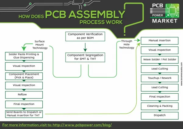
Printed Circuit Board (PCB) assembly is at the heart of every electronic device we use—from smartphones and computers to home appliances and medical equipment. While the final product might look simple, the process of assembling a PCB is complex and precise. In this blog, we’ll break down the step-by-step process of PCB board assembly, helping you understand how raw boards transform into fully functioning electronics. Step 1: Design and Schematic Preparation Before any assembly can begin, a detailed PCB design is created using CAD software. The schematic includes the layout, component placement, and routing of electrical connections. This design is then translated into Gerber files, which are essential for manufacturing and PCB board assembly. Step 2: Solder Paste Application In Surface Mount Technology (SMT), the process starts with applying solder paste to the board. A stencil is placed over the PCB, and solder paste is spread across the stencil to deposit small amounts of paste on the pads where components will be placed. Step 3: Component Placement
Next, pick-and-place machines are used to accurately position surface mount components on the board. These automated machines read the design files and quickly place each part on the solder-pasted areas with high precision. Step 4: Reflow Soldering Once components are in place, the PCB is passed through a reflow oven. The oven heats the solder paste until it melts and forms a solid bond between the component leads and the PCB pads. The board is then gradually cooled to solidify the connections. Step 5: Inspection and Quality Control Post-reflow, the assembly goes through Automated Optical Inspection (AOI) to check for misaligned components, soldering defects, or missing parts. For more complex or high- reliability boards, X-ray inspection may be used to verify connections under components like BGAs (Ball Grid Arrays). Step 6: Through-Hole Component Insertion (If Applicable) If the design includes through-hole components, they are inserted into the board manually or with an automated insertion machine. These components are then soldered using wave soldering or manual soldering, depending on the project. Step 7: Functional Testing Once assembly is complete, the board undergoes electrical and functional testing to ensure all components work as intended. Tests may include in-circuit testing (ICT), boundary scan, or full functional testing depending on complexity and application. Step 8: Final Cleaning and Packaging After testing, the assembled PCB is cleaned to remove flux residues and any contaminants. It’s then dried, inspected one final time, and packaged safely for delivery or further integration into the final product. Final Thoughts PCB board assembly is a meticulous process combining engineering, automation, and quality control. Whether you're a hobbyist or managing large-scale manufacturing, understanding each step helps ensure better design choices and smoother production.