Download
1 / 23
230 likes | 343 Views
A detailed overview of the RAMP Blue architecture including project goals, design principles, implementation experience, and future work. Explore processor infrastructure, network interface, FPU, and software support. See how the system supports running uClinux and real MPI benchmarks on a cluster of MicroBlaze cores.

E N D
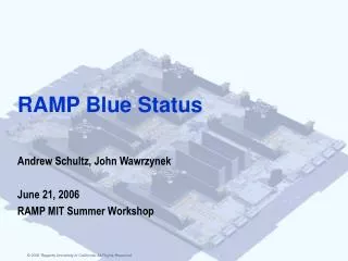
RAMP Blue Status Andrew Schultz, John Wawrzynek June 21, 2006 RAMP MIT Summer Workshop
Contributors • Andrew Schultz • Dave Patterson, and the Spring 2006 CS252 (grad computer architecture) class: Mitch Harwell David Tylman Xiaofen Jiang Neelima Balakrishnan Khang Tran Matt Brockmeyer Marghoob Mohiyuddin Jue Sun Zhangxi Tan Wei Xu Gary Voronel Luke Beamer
Outline • Review of project goal and requirements • RAMP Blue Architecture • Design principles • Processor infrastructure • Network interface and on-chip switch • Double precision floating point • Software support • Implementation experience • Future work
Project Goal and Requirements • Goal:1000 node cluster of MicroBlaze cores running uClinux and real MPI benchmarks • Requirements: • Infrastructure to boot uClinux on MicroBlaze cores situated on BEE2 user FPGAs • Double precision floating point unit for real MPI benchmarks • On-chip switch capable of routing packets between FPGAs on and off module • Port of message passing framework (MPI, UPC, etc.)
2VP70 FPGA 2VP70 FPGA 2VP70 FPGA 2VP70 FPGA 2VP70 FPGA BEE2 Module Design • Per-module: • 5 Virtex-IIPro70 FPGAs • 20GB DRAM • 20 10Gbps connections • Supports 10GigE/Infinibnd • System I/O • Inter-mod connections • RAMP-blue • maps target MBs to four “user” FPGAs, and hard PowerPC on “control” FPGA as host maintenance processor.
Andrew’s Design Principles • KISS: We tried to keep everything simple. Don’t over-engineer the network, FPU, or infrastructure until we have a working design. • Share the wealth: Resources are tight and MicroBlazes are wimpy. Share infrastructure such as interchip pins, memory controllers, and even FPUs. • Cut the fat: Wherever possible take care to remove unnecessary logic and interfaces not required by MicroBlaze in this context. • FSL everywhere: FSL is simply FIFO based communication (very similar to very basic RAMP channel). Ease routing and provide easy migration to RDL
Console network serves several purposes Download application/kernel from control FPGA Provide terminal to booted uClinux Network conduit to route packets from MB to control FPGA (or even off board via 10/100 Ethernet) Simple, general purpose, FSL based network with OPB FIFO attachment at PPC Linux driver for TTY, char device, and Ethernet abstraction Console Network
MB/MB Network Interface • Current network interface is raw FSL connected directly to a on-chip switch • Interrupt driven, programmed I/O approach • Simple Linux driver provides Ethernet interface so applications can utilize network via tradition socket interface • Very inefficient, yet very simple for first network implementation • Discussion and paper design of second generation network interface • Direct memory access through direct port to memory controller • Possible RDMA support for UPC as well
Switch provides drop-free transmission of variable length packets from MB to MB Composed of two units: buffer unit and switch Buffer unit provides buffering at each hop and address lookup logic Switch provides cross-bar connectivity between input ports and output ports and arbitration for each port Packets are source routed (currently encapsulated Ethernet packets) CRCs are end-to-end, so end-points must manage retransmits or fail-stop On-Chip Switch
Double Precision FPU • FPU is treated as a co-processor • Investigation into integrating FPU with RF as SP FPU does was too complicated and didn’t facilitate sharing • Operands are transferred via FSL in four instructions, and MB blocks for result • FPU is highly pipelined so to better utilize it makes sense to share (and saves loads of resources)
Initial FPU Performance 2D FFT (ffbench) Execution Times MicroBlaze FP emulation Mitch Harwell & David Tylman MicroBlaze DP FPU Sun 386/250
Main Memory • Clusters of MBs share a single physical DIMM (1GB) • Memory is partitioned so each core has its own physical address space
Other Infrastructure • Bootstrapping: Reduced boot-strap block RAM from four to one and fit simple boot-loader and cache-invalidation code in single, read-only BRAM. • Peripherals: Remove the OPB bus and port interrupt controller and timer to LMB to save logic. Pending. • Debugging: Using existing opb_mdmcore and JTAG we can use existing debugging infrastructure (i.e. XMD/GDB) to debug up to 8 cores. Group of students also worked on ideas for real time instruction tracing.
Software Support • MBs boots relatively unmodified version of uClinux and runs stably • MPICH2 has been successfully compiled and run on an XUP test system with a pair MicroBlaze cores • UPC has also been built and run on a XUP test system • GCC has been modified to emit instructions that utilize double precision FPU co-processor (when SOFTFPU flag turned on) • Currently finishing up final modifications to first network driver to allow proper source routing of packets between FPGAs and to other BEE2 boards
Implementation Experience • System with 8 MicroBlaze cores per user FPGA running on the BEE2 • This system has the integrated SP FPU per core, we haven’t yet integrated DP FPU core into this base system, although we expect fewer resources with sharing (each SP FPU is ~1300 slices and the DP FPU is ~2000 slices) • Early attempts to implement a 16 MicroBlaze system have failed in placement, although there are enough raw resources • We expect that with some simple floor planning we should be able to reach a 16 core system
8 MicroBlaze Cores (SP FPU each) 4 Memory Controllers 4 XAUI Controllers 4-LUTs: 40,625 out of 66,176 61% FFs: 27,085 out of 66,176 40% BRAMs and MULTs: 116 out of 328 35% 56 out of 328 17%
Near-term Work • Improve density to get 16 core system • Analysis of data paths and floor planning should allow us to increase the density of cores since current design does very little deliberate area optimization • Integrate shared DP FP core • Convert design to RDL • Present design is XPS only (however it is fully parametrized with embedded TCL to allow fast changes to topology) • Have version of network switch in RDL, need to wrap the rest in RDL • Improve performance of known bottlenecks • Second generation NIC with direct memory access to take load off MB • Add buffering of FPU operands to allow single cycle sharing of FPU
Processor Infrastructure • Key components are required for each processor • MicroBlaze core • Console interface • Network interface • Floating point unit • Memory interface • Debug port • Miscellaneous infrastructure (timer, interrupt controller) • Build one and then replicate, connect with on-chip switch
Farther Future Work • System level possibilities? • Hardware paging of memory (ala VMWare ESX) to better utilize memory capacity and allow content based sharing • Coherent shared memory between MicroBlazes • More exploration of tracing and system level debugging • Networking possibilities? • Highly FPGA optimized switch • More complicated routing mechanisms
Conclusion • Close to functional multi-MB system: • Successfully provided infrastructure to boot multiple MicroBlaze cores on single FPGA with full uClinux support • Determined ease of porting and running MPI and UPC on uClinux • Areas targeted for both performance increase (network interface, FPU integration) and on-chip density