Download
1 / 9
90 likes | 237 Views
Cascaded BCD Counter and Display Specification.

E N D
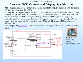
Cascaded BCD Counter and Display Specification Aim : Capture, simulate and implement a 2-digit, loadable BCD up/down counter, with chip enable I/P (CE) and chip enable O/P (CEO). Implement on the Digilent Xilinx Spartan-3 FPGA development system. Display the two digit count value on the two least significant 7-segment displays. Display the two digit counter load values on the two most significant MSB 7-segment displays. Assume a 50MHz system clk frequency. Internally, generate a one-clk-period duration enable pulse every second (every 50M, [maxCount] clock cycles and use to gate the chip enable input (CE input). ISE module VHDL file name is d3Design.vhd Use component displayCtrlr to display the current counter digits value and the counter load value input Digilent Spartan-3 Xilinx FPGA hardware development system displayCtrlr 3.0
Contents • This document contains: • Submission / demonstration instructions • Top level d3Design Context Diagram, Data Dictionary and FPGA Pinout • cascadedBCDCntr Functional Partition • cascadedBCDCntr count algorithm and CEO function pseudo code • Description of ISE project template files provided • lab instructions • Reference timing diagrams (simulation waveforms)
Top level d3Design Context Diagram, Data Dictionary and FPGA Pinout • clk: input strobe, 50 MHz • rst: asynchronous reset input. Assertion (H) clears all system registers • d(7:4): most significant counter digit load data. Connected to FPGA board toggle switch inputs sw(7:4) • d(3:0): least significant counter digit load data. Connected to FPGA board toggle switch inputs sw(3:0) • load: counter load input signal. Assertion synchronously loads values d(7:4) and d(3:0) into counter upper and lower digits respectively. Connected to FPGA board spring loaded switch input btn(2) • uD: counter up/down input signal. Assertion/deassertion defines up/down counter functionality. Connected to FPGA board spring loaded switch input btn(1) • ce: counter chip enable input signal. Assertion activates the counter. Connected to FPGA board spring loaded switch input btn(0) • ld(7:0): signals driving LEDs. Apply a fixed pattern • seg7L(6:0): low asserted 7 segment LED signals. ‘0’ lights each LED. Display the two digit count value on the two least significant 7-segment displays. Display the two digit counter load values on the two most significant MSB 7-segment displays. • anL(3:0): low asserted 7-segment display anode control. d3Design Component symbol
cascadedBCDCntr algorithm and ceoProc (pseudo code) This is not correct VHDL syntax (intended as aid only) Use integers in counter description (lwrInteger, uprInteger) Use VHDL vector-to-integer and integer-to-vector conversion functions if rst = ‘1’ then o/ps are cleared else if active clk edge then if load = ‘1’ then assign lwrInteger and uprInteger to integer representation of d(7:0) elsif ce = ‘1’ then if uD = ‘1’ then – counting up if lwrInteger < 9 then increment lwrInteger else lwrInteger <= 0; if uprInteger < 9 then increment uprInteger else uprInteger = 0; end if; end if; else – counting down repeat above for down count function end if; end if; end if; ceoProc: ceo <= ‘0’ – default ceo <= ‘1’ when ce = ‘1’ and uprInteger=9 and lwrInteger=9 and ud=‘1’ or uprInteger=0 and lwrInteger=0 and ud=‘0’
Description of ISE project template files provided Project file User constraints file including FPGA pinout assignment cascadedBCDCntr&Display synthesisable VHDL model (template code provided, to be completed) Simulation automatic macro (provided)Simulation user macro (provided)VHDL Testbench (provided)Modelsim preferences file (Provided) Review and become familiar with all of the above filesProject level definitions/components declared inNUIGPackage.vhd (NUIGPackage)
Lab instructions Xilinx ISE Project : cascadedBCDCntr&Display.ise Provides access to all of the constituent files P1: VHDL capture and simulation • Complete d3Design.vhd VHDL model template to fully describe the required model. Process labels are included corresponding to the labels on the functional partition • The displayCtrlr component is included in the d3Design.vhd • Check VHDL code syntax, synthesise and view RTL schematic. • Review the VHDL testbench code (d3Design_TB.vhd) and Modelsim macro files provided. Simulate fully, review timing waveform, verify VHDL model operation. P2: Implement on FPGA • Review d3Design.ucf (provided) for pinout • Implement d3Design.vhd top level model and test
Reference Timing Diagrams Simulation waveforms (d3Design level)
Reference Timing Diagrams Simulation waveforms (zoomed in), (d3Design level)