Download
1 / 69
710 likes | 963 Views
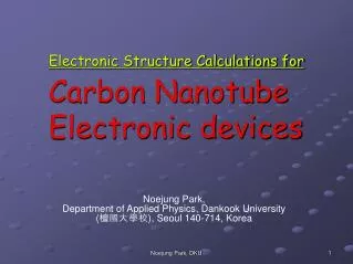
0. Electronic Structure Calculations for Carbon Nanotube Electronic devices. Noejung Park, Department of Applied Physics, Dankook University ( 檀國大學校 ), Seoul 140-714, Korea. Samsung Advanced Institute of Technology (Dr. Wanjun Park, Dr. Yosep Min…)

E N D
0 Electronic Structure Calculations forCarbon Nanotube Electronic devices Noejung Park, Department of Applied Physics, Dankook University (檀國大學校), Seoul 140-714, Korea Noejung Park, DKU
Samsung Advanced Institute of Technology (Dr. Wanjun Park, Dr. Yosep Min…) Korea Research Institute of Standards and Science ( Dr. Jinhee Kim, Dr. Woon Song…) Korea Research Institute of Chemical Technology ( Dr. Jeong-O Lee…) Sejong University (Prof. Suklyun Hong, Mr. Dongchul Sung ) 0 Contributions from Noejung Park, DKU
Computational Method • First-principels calculations with the Density Functional Theory • Vienna Ab inito Simulation Package, PAW GGA (PAW_PBE) Noejung Park, DKU
Carbon Nanotube • Semiconductor or Metal, depending on V = n*a1 + m*a2 • Long and thin (aspect ratio ~ 1000) • Excellent thermal and electronic conduction • Mechanically strong and chemically stable. Noejung Park, DKU
SemiconductingCNT S D Dielectric Gate Vg Field Effect Transistor Noejung Park, DKU
Various device structures Infineion Technology Noejung Park, DKU
Potential Applications Memory Nonvolatile memory, Nantero Noejung Park, DKU
Potential Applications Logic circuit Huang et al., Science (01) Noejung Park, DKU
Potential Applications Sensor Device J.-O.Lee & N.Park (06) Noejung Park, DKU
Nanotube transistors are commonly p-type ? “n-type” is required for CMOS-like operations. Channel and contact are not clearly separated. Short Channel Single Clean CNT 0 Please remember… Noejung Park, DKU
S D Dielectric Gate Isd Isd Vg Vg p-type n-type 0 n-type or p-type Noejung Park, DKU
Invertor Noejung Park, DKU
(Q) Why p-type FET is so common ? (A) Metal electrode itself induces the Hole doping or lower Schottky barrier. 0 Question and Answer Noejung Park, DKU
S D Dielectric Gate Where is the Metal-CNT interface ? Noejung Park, DKU
{Al, Au }/CNT interface (10,0)CNT Al Au Park and Hong, Phys. Rev. B 74, 045408(2005). Noejung Park, DKU
{Bare Al} vs. {oxidized Al} Park and Hong, Phys. Rev. B 74, 045408(2005). Noejung Park, DKU
Oxidation Work function increase ~ 1 eV Park and Hong, Phys. Rev. B 74, 045408(2005). Noejung Park, DKU
Al nanoparticles deposition hole doping {▼Oxidized Aluminium} Right-shift of Ids-Vg Metal Metal Au Gate dielectric Gate B-K. Kim, JO Lee,N. Park Nanotechnology Noejung Park, DKU
0 Answer p-type n-type p-type Al Au Noejung Park, DKU
0 Answer • It’s not easy to fabricate the ‘n-type’-favorable contact !!! • “Charge-transfer doping” by metal electrode itself • Small work function metals are vulnerable to oxidations Noejung Park, DKU
Experimental Success : Al sputtering with high vacuum n-type FET Hwangyou Oh, JH Kim, and N Park, Appl. Phys. Lett. Noejung Park, DKU
Al deposition without oxidation could lead to n-type FET !!! H. Oh et al. and N. Park Appl. Phys. Lett. (2006) Noejung Park, DKU
Then, Does “large work function metal” always lead to p-type ? 0 Question again… Noejung Park, DKU
According to Leonard & Tersoff(00), Electrostatics tells that the “large work function metal” should always lead to p-type !!! 0 Suggestions by others Widespread misunderstandings Noejung Park, DKU
Please remember …………. Bulk Metal and very narrow semiconductor Noejung Park, DKU Lin et al, NanoLetters2004
“Fermi level pinning”, a text book review Semiconductor Metal Schottky barrier for n-type semiconductor X Neamen, Semiconductor Physics and Devices Noejung Park, DKU
Irrespective of the metal work function, the Fermi level is pinned to somewhere in the midgap ! Noejung Park, DKU
0 Common understanding of metal-CNT contact CNT or a very thin semiconductor Metal • Irrespective of the contact details • Practically No pinning • Schottky barrier = Noejung Park, DKU
Phys. Rev. B 69, 161402(2004). Noejung Park, DKU
Metal-semiconductor 2D contact Large Work Function Metal Semiconductor Weak pinning Strong pinning Noejung Park, DKU Leonard and Tersoff, PRL84, 4693(2000)
Metal-CNT contact Nanotube Weak pinning Metal Strong pinning Noejung Park, DKU Leonard and Tersoff, PRL84, 4693(2000)
Strong pinning No pinning FSB FSB Ef Ef Noejung Park, DKU
Effectively No pinning, irrespective of the interface coupling. • “Large work function metals” always leads to p-type FET. Noejung Park, DKU
Strong Fermi level pinning at M-CNT interfaces in some cases. The “large work function metal” does not necessarily lead to p-type !!! 0 Our Suggestion Noejung Park, DKU
Au/CNT, Ef pinning at the midgap Noejung Park, DKU
Al/CNT, Ef pinning at the midgap Relaxed Latt=14.882Å, Intertube=7.9Å Noejung Park, DKU
1.0nm Ef Pinning throughout the whole CNT MIGS Noejung Park, DKU
0 Partial Summary • Strong M-C bonds formation induces the strong Fermi level pinning !!! • Not only the metal work function, but the effect of the local dipole at the interface is also significant !! Noejung Park, DKU
The more interesting M-C interface. No chemical bond, but with a pressure Metal Metal Au Dielectric Gate Noejung Park, DKU
Gold/CNT contact Z (a) Park et al. APL 87, 013112(2005) Noejung Park, DKU
[skip] Compressed CNT, band structure (c) (b) (d) Park et al. APL 87, 013112(2005) Noejung Park, DKU
Charge density profile Noejung Park, DKU
Embedded CNT has more positive charge and lower potential Metal Metal CNT CNT Noejung Park, DKU
Model for the pressure on the embedded CNT Noejung Park, DKU
Embedded CNT under W layer. Wei et al., Ultramicroscopy 85,93(2000) Noejung Park, DKU
0 Partial Summary • A large work function metal could show an ambipolar or even n-type conduction behavior !! Noejung Park, DKU
Au Au Au Gate dielectric Gate n-type FET with large work function metal Gold/CNT contact Pressure Heinze et al., Phys. Rev. Lett. 2002 Derycke et al., Appl. Phys. Lett. 2002 Noejung Park, DKU
KRISS (Dr. Jinhee Kim) Noejung Park, DKU
0 Co/Au electrode • Some devices show p-type, some others show ambipolar or even n--type operations. • The difference should be attributed to the difference in M-CNT interfaces. Noejung Park, DKU
Then, Why the p-type is so common ? 0 Come back to the Question Noejung Park, DKU