Download
1 / 12
130 likes | 733 Views
Dip-pen Nanolithography. Yu Shi Dept. of Materials Science & Engineering. From microscopy to lithography. Scanning probe microscope. electron microscope. optical microscope. ?. photolithography. E-beam lithography. 10 -5 m. 10 -6 m. 10 -7 m. 10 -8 m. 10 -9 m. 10 -10 m. 10 -11 m.

E N D
Dip-pen Nanolithography Yu Shi Dept. of Materials Science & Engineering
From microscopy to lithography Scanning probe microscope electron microscope optical microscope ? photolithography E-beam lithography 10-5m 10-6m 10-7m 10-8m 10-9m 10-10m 10-11m If you can see, then you should be able to write…
History and origin 4,000 years ago… Invention of AFM in 1986… 1995 by Jaschke & Butt… 1999… Butt et al. Langmuir 11, 1061 (1995). Mirkin et al. Science 283, 661 (1999).
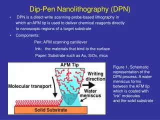
Principle Source: http://www.nanoink.net
Principle Mirkin et al. Science 283, 661 (1999).
Extended capabilities I Mirkin et al. Nature Nanotechnology 2, 145 (2007).
Extended Capabilities II 55,000 cantilevers and 88,000,000 gold dots! Mirkin et al. Nature Nanotechnology 2, 145 (2007).
Compare & contrast Source: http://www.nanoink.net
Thank you! Q & A…
Idea from Mirkin • “DPN is finding applications in certain areas that impact the semiconductor industry such as mask fabrication, inspection and repair…” • “…However, its unique attributes have positioned it on a different path aimed largely at exploiting the properties and applications of nanopatterned soft materials…” -- C. A. Mirkin (2007) Mirkin et al. Nature Nanotechnology 2, 145 (2007).