Nanolithography
Nanolithography. Lecture 15 G.J. Mankey gmankey@mint.ua.edu. Writing and Printing. To go far beyond the Raleigh limit of optical processes, other probes must be applied.


Nanolithography
E N D
Presentation Transcript
Nanolithography Lecture 15 G.J. Mankey gmankey@mint.ua.edu
Writing and Printing • To go far beyond the Raleigh limit of optical processes, other probes must be applied. • By definition a nanostructure is one with nanometer dimensions, but in practice true nanoscience implies a paradigm shift of the lithography process to below 100 nm. • Sub 100-nanometer writing and printing requires the use of x-rays, electron beams, focused ion beams, atomic force probe tips, or a nanoimprint mask. • Printing processes are x-ray lithography and nanoimprint lithography. • The writing processes all involve scanning the probe across the surface writing a single spot at a time and are thus time consuming and expensive.
Why Nano? • Semiconductors and magnetic storage devices will get smaller. • A current bit on a hard drive is 300 nm by 100 nm. • The future evolution of this technology will require nanoscale readers, writers and possible media. • To be marketable, these devices must be inexpensive and reliable. • The challenge for physics is not only to make it possible, but routine! ref: W. Eberhardt in Frontiers in Surface and Interface Science (2002).
The wavelength of an electron is The diffraction limited beam has a diameter d = 0.6l/a, where a is the beam divergence (~0.01). A 10 kV beam has l = 0.01 nm and this simple analysis gives a 1 nm spot. In general, the spot sizes are added in quadrature, as shown in the diagram. Resolution Limit of e-beams ref: Handbook of Microlithography, Micromachining and Microfabrication, SPIE (1997)
Electron-Solid Interactions • Increasing electron beam energy arbitrarily will not result in a smaller spot in the resist. • Higher energy electrons produce more secondary electrons which travel through the solid and expose a larger volume of resist. • This is similar to photoelectron blur in x-ray lithography which ultimately puts a limit on the smallest achievable feature. • Features ~ 10 nm are theoretically possible, but rarely demonstrated. ref: Handbook of Microlithography, Micromachining and Microfabrication, SPIE (1997)
Two Layer Resist Processing • The best results of e-beam have been achieved for making a pattern of a single layer of evaporated or sputtered material. • The two-layer process produces an undercut structure which functions as a shadow mask for the deposition process. • After deposition from a collimated source, the resist is removed with a solvent. ref: Handbook of Microlithography, Micromachining and Microfabrication, SPIE (1997)
Resist Contrast High Contrast Low Contrast D1 • Resist contrast determines sensitivity to process parameters such as exposure time and resist thickness. • Higher contrast resist usually has a more vertical sidewall angle. • The contrast is defined as: Film Retention (%) D2 Log (Electron Dose) ref: Handbook of Microlithography, Micromachining and Microfabrication, SPIE (1997)
P = 40 nm P = 45 nm P = 50 nm P = 60 nm Dot Arrays Fabricated by EBL • AFM images of dot arrays of different period fabricated by e-beam lithography, followed by thermal evaporation and lift-off. • The pitch, P, is varied systematically while the raster rate and beam current are constant. • Under the experimental conditions, uniform arrays are obtained when the period is greater than 45nm. The density of the dots is up to 300 Gdot/in2. • Image size is one square micrometer.
X-Ray Lithography • X-rays are produced by synchrotron radiation from a bending magnet in a high energy electron storage ring. • Resist, usually PMMA, is exposed through an x-ray mask in proximity or in contact with the wafer. • This technique has the advantage that very high aspect ratios can be achieved, since the x-rays are highly penetrating. ref: Handbook of Microlithography, Micromachining and Microfabrication, SPIE (1997)
Resolution Limit of XRL • The wavelength of an x-ray is given by l = 1.2/E(keV), so one would expect higher energies to be more desirable. • Blur, caused by the excitation of photoelectrons and the associated shower of secondary electrons limits the patterning ability to about 20 nm. • XRL has been applied to MEMS, where the high aspect ratio is a distinct advantage. ref: Handbook of Microlithography, Micromachining and Microfabrication, SPIE (1997)
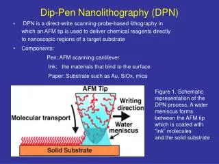
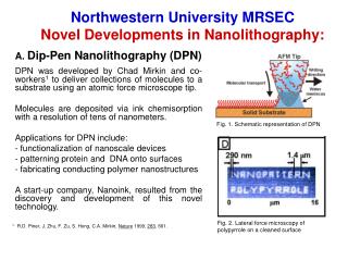
AFM Lithography • The AFM tip is used to "bulldoze" through a top layer of resist. • Submersion in developer produces an undercut in the lower layer of resist. • The top layer then serves as a shadow mask for deposition. • After removal of resist, the deposited nanostructure remains. • For nanocontact printing, the initial structuring is performed in parallel with a contact mask. Undercut Developing AFM Bulldozing Depositing Lift Off