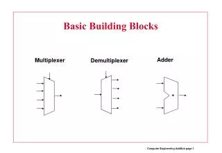
Review: Basic Building Blocks
This review explores the fundamental building blocks of memory architectures, focusing on SRAM and DRAM technologies. Key features of SRAM include fast, static storage with a minimum of 6 transistors per cell, while DRAM utilizes smaller cells requiring periodic refresh. The analysis covers aspects such as read-write operations, voltage ratios, and the design of sense amplifiers. Readers will gain insight into the importance of cell sizing, the impact of capacitance on performance, and various memory types' practical applications in modern computing systems.

Review: Basic Building Blocks
E N D
Presentation Transcript
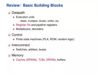
Review: Basic Building Blocks • Datapath • Execution units • Adder, multiplier, divider, shifter, etc. • Register file and pipeline registers • Multiplexers, decoders • Control • Finite state machines (PLA, ROM, random logic) • Interconnect • Switches, arbiters, buses • Memory • Caches (SRAMs), TLBs, DRAMs, buffers
Review: Read-Write Memories (RAMs) • Static – SRAM • data is stored as long as supply is applied • large cells (6 fets/cell) – so fewer bits/chip • fast – so used where speed is important (e.g., caches) • differential outputs (output BL and !BL) • use sense amps for performance • compatible with CMOS technology • Dynamic – DRAM • periodic refresh required • small cells (1 to 3 fets/cell) – so more bits/chip • slower – so used for main memories • single ended output (output BL only) • need sense amps for correct operation • not typically compatible with CMOS technology
Review: 4x4 SRAM Memory read precharge 2 bit words bit line precharge enable WL[0] !BL BL A1 WL[1] Row Decoder A2 WL[2] WL[3] Column Decoder A0 clocking and control sense amplifiers write circuitry BL[i] BL[I+1]
6-transistor SRAM Cell WL M2 M4 Q M6 M5 !Q M1 M3 !BL BL
SRAM Cell Analysis (Read) WL=1 M4 M6 !Q=0 M5 Q=1 M1 Cbit Cbit !BL=1 BL=1 Read-disturb (read-upset): must carefully limit the allowed voltage rise on !Q to a value that prevents the read-upset condition from occurring while simultaneously maintaining acceptable circuit speed and area constraints
SRAM Cell Analysis (Read) WL=1 M4 M6 !Q=0 M5 Q=1 M1 Cbit Cbit !BL=1 BL=1 Cell Ratio (CR) = (WM1/LM1)/(WM5/LM5) V!Q = [(Vdd - VTn)(1 + CR (CR(1 + CR))]/(1 + CR)
Read Voltages Ratios Vdd = 2.5V VTn = 0.5V
SRAM Cell Analysis (Write) WL=1 M4 M6 !Q=0 Q=1 M5 M1 !BL=1 BL=0 Pullup Ratio (PR) = (WM4/LM4)/(WM6/LM6) VQ = (Vdd - VTn) ((Vdd – VTn)2 – (p/n)(PR)((Vdd – VTn - VTp)2)
Write Voltages Ratios Vdd = 2.5V |VTp| = 0.5V p/n = 0.5
Cell Sizing • Keeping cell size minimized is critical for large caches • Minimum sized pull down fets (M1 and M3) • Requires minimum width and longer than minimum channel length pass transistors (M5 and M6) to ensure proper CR • But sizing of the pass transistors increases capacitive load on the word lines and limits the current discharged on the bit lines both of which can adversely affect the speed of the read cycle • Minimum width and length pass transistors • Boost the width of the pull downs (M1 and M3) • Reduces the loading on the word lines and increases the storage capacitance in the cell – both are good! – but cell size may be slightly larger
6T-SRAM Layout VDD M2 M4 Q Q M1 M3 GND M5 M6 WL BL BL
WL2 WL1 M2 M4 M5 !Q Q M6 M7 M8 M1 M3 !BL2 !BL1 BL1 BL2 Multiple Read/Write Port Cell
4x4 DRAM Memory read precharge 2 bit words bit line precharge enable WL[0] BL A1 WL[1] Row Decoder A2 WL[2] WL[3] sense amplifiers clocking, control, and refresh BL[0] BL[1] BL[2] BL[3] write circuitry A0 Column Decoder
write WWL Vdd BL1 X Vdd-Vt RWL read Vdd-Vt BL2 V 3-Transistor DRAM Cell WWL RWL M3 X M1 M2 Cs BL2 BL1 No constraints on device sizes (ratioless) Reads are non-destructive Value stored at node X when writing a “1” is VWWL - Vtn
3T-DRAM Layout BL2 BL1 GND RWL M3 M2 WWL M1
1-Transistor DRAM Cell WL write “1” read “1” WL X M1 X Vdd-Vt Cs CBL Vdd BL Vdd/2 BL sensing Write: Cs is charged (or discharged) by asserting WL and BL Read: Charge redistribution occurs between CBL and Cs Read is destructive, so must refresh after read
DRAM Cell Observations • DRAM memory cells are single ended (complicates the design of the sense amp) • 1T cell requires a sense amp for each bit line due to charge redistribution read • 1T cell read is destructive; refresh must follow to restore data • 1T cell requires an extra capacitor that must be explicitly included in the design • A threshold voltage is lost when writing a 1 (can be circumvented by bootstrapping the word lines to a higher value than Vdd)

