Download
1 / 6
60 likes | 165 Views
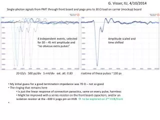
G. Visser , IU, 4/10/2014. Single-photon signals from PMT through front board and pogo pins to 30 Ω load on carrier (mockup) board. 4 independent events, selected for 30 – 45 mV amplitude and “no obvious extra pulses”. Amplitude scaled and time shifted.

E N D
G. Visser, IU, 4/10/2014 Single-photon signals from PMT through front board and pogo pins to 30 Ω load on carrier (mockup) board 4 independent events, selected for 30 – 45 mV amplitude and “no obvious extra pulses” Amplitude scaled and time shifted 20 GS/s 500 ps/div 5 mV/div ext. att. 0.83 risetime of these pulses ~130 ps • My initial guess for a good termination impedance was 70 Ω – not so good • The ringing that remains here • Is just the linear response of connection parasitics, same on every pulse, harmless • Might be improved with a series resistor on the front board capacitors, and/or an isolation resistor at the −600 V pogo pin on HVB to be explored on 2nd HVB/front
other pictures at http://npvm.ceem.indiana.edu/~gvisser/BelleII/iTOP/boardstack_and_SK-35/
First attempt w/ 2-stage amp on “carrier” board. I suspect the severe ringing is due to new 30 Ω scheme, and can be resolved. But this only got working about 20 minutes ago. Needs a bit more time. 640 psrisetime good (too fast?) HVB @ 3200 V here
Updated update, 4/11/2014 The severe ringing issue in previous results seems to be related to the LMH6629 input stage reacting to the fast pulse (which is well beyond the LMH6629 closed-loop bandwidth, but perhaps within the input stage’s open-loop bandwidth). “Fixed” now, with an R-C filter at the very input. (In quotes because a fix which we don’t fully understand isn’t fully satisfying. But it may have to do.) HVB input 3200 V risetime 750 ps Amplifier VCC = 3.6 V load = 10 pF gain = 3188 Ω (calc.) 20 GS/s 2ns/div 100 mV/div
Noise and bandwidth look reasonable. As before, the load capacitance is an important noise-filter component; explicit capacitor should be included at IRSX input on Carrier Rev. E, value TBD. [I suggest also on the test board.] [UH: Do you guys have a network analyzer? If so could you measure input on test board please?] • HVB off • all else exactly as before • −50 dBm 141 nV/sqrt(Hz) • input referred: • 1.54 nV/sqrt(Hz) • It’s about the expected value, and a respectable figure IMHO. no load 10 pF inst. noise floor 250 MHz/div 3 dB/div RBW=25 MHz
Revised circuit, basically as was used for these latest tests. • Output probe buffer not shown • Actual board has C4 to VREF not ground (better layout, should be equivalent) • Actual board has 10nF caps (what I have right now) • Expect some further tweaking, perhaps adding an inductor at input and/or output • Cal circuit feeds into 2nd stage as summer, not shown here Note: Compensation selector (pin 6) is just a logic signal. It is wired as shown to optimize the layout. It’s on my to-do list to verify PSRR from C pin is good i.e. well beyond V+ pin spec. Or else, this plan will change.